MEMS (Micro Electro Mechanical System) piezoresistive type absolute pressure sensor based on SOI (Silicon on Insulator) silicon chip

An absolute pressure, piezoresistive technology, applied in piezoelectric devices/electrostrictive devices, processes for producing decorative surface effects, piezoelectric/electrostrictive/magnetostrictive devices, etc., which can solve the overload resistance capability Limited, low overload resistance, etc., to achieve the effects of good performance, high yield, and reasonable structural design

Inactive Publication Date: 2015-04-15
PEKING UNIV
View PDF5 Cites 1 Cited by
  • Summary
  • Abstract
  • Description
  • Claims
  • Application Information

AI Technical Summary

Problems solved by technology

Due to the existence of the strain film, limited by the fracture strength of the silicon material, the traditional piezoresistive pressure sensor has limited anti-overload ability, and the piezoresistive pressure sensor in the application field of high pressure has the disadvantage of low anti-overload ability.

Method used


Image

  • MEMS (Micro Electro Mechanical System) piezoresistive type absolute pressure sensor based on SOI (Silicon on Insulator) silicon chip
  • MEMS (Micro Electro Mechanical System) piezoresistive type absolute pressure sensor based on SOI (Silicon on Insulator) silicon chip
  • MEMS (Micro Electro Mechanical System) piezoresistive type absolute pressure sensor based on SOI (Silicon on Insulator) silicon chip

Examples


Embodiment Construction

[0032] The present invention will be further described below through specific embodiments and accompanying drawings.

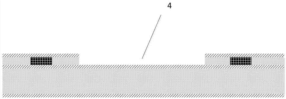
[0033] In the manufacturing method of the MEMS piezoresistive pressure sensor of this embodiment, piezoresistors are manufactured on the four side walls of the shallow rhombic groove by ion implantation after etching the shallow rhombic groove on the surface of the silicon wafer. The steps of the method include:

[0034] 1) Choose (100) SOI (silicon on insulator) silicon wafer as the chip substrate;

[0035] 2) Fabricate a P-type heavily doped contact region by ion implantation on the front side of the substrate, and activate the implanted impurities by high-temperature thermal annealing after completion;

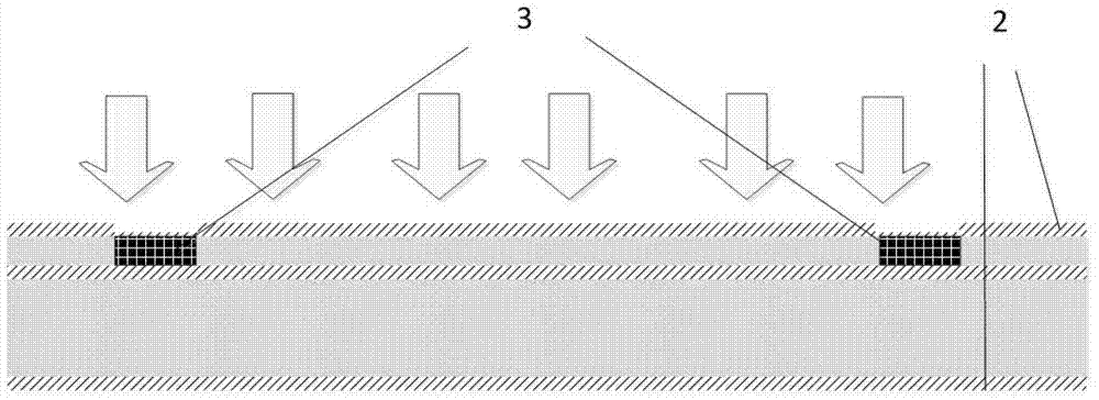
[0036] 3) Define the shape of the front shallow groove by photolithography, and make the shallow groove by reactive ion etching; after completion, high temperature thermal annealing is used to activate the implanted impurities;

[0037] 4) Fabricate piezo...


PUM


Abstract

The invention provides an MEMS (Micro Electro Mechanical System) piezoresistive type absolute pressure sensor based on an SOI (Silicon on Insulator) silicon chip, which comprises a substrate provided with a quadrilateral slot and four groups of piezoresistors manufactured on the side wall of the slot, wherein the four groups of piezoresistors form a Wheatstone bridge; the two opposite side walls of the quadrilateral slot are arranged along a crystal orientation (100) of the substrate, and the other opposite side walls of the quadrilateral slot are arranged along a crystal orientation (101) of the substrate. The MEMS piezoresistive type absolute pressure sensor comprises the following manufacturing steps: photoetching and defining a P type heavily-doped lead contact area on the front surface of the substrate for ion implantation and high-temperature thermal annealing; photoetching and defining the shape of the slot on the front surface of the substrate and etching the quadrilateral slot; doping the piezoresistors on the side walls through P type ion implantation light doping and carrying out high-temperature thermal annealing; manufacturing a lead hole and a metal lead; and scribing. The MEMS piezoresistive type absolute pressure sensor has the beneficial effects that no strain film is contained, the chip size of the sensor can be reduced, the anti-overload capacity of the sensor is remarkably increased, and the process reliability and the device yield are improved.

Description

technical field [0001] The invention belongs to the field of micro-electro-mechanical system (MEMS) sensor design, and relates to a MEMS piezoresistive absolute pressure sensor and a method for manufacturing the pressure sensor on a single wafer using a MEMS processing technology. Background technique [0002] MEMS (Micro Electro Mechanical System) is an emerging interdisciplinary high-tech research field. The piezoresistive pressure sensor based on MEMS technology has been widely used in the modern market due to its excellent accuracy and reliability and relatively cheap manufacturing cost. Silicon-based piezoresistive pressure sensors have been widely used since the discovery of the piezoresistive properties of silicon materials in the mid-1950s. The working principle of a typical piezoresistive pressure sensor is to make four pressure-sensitive resistors in the stress concentration area by diffusion or ion implantation on a square or circular silicon strained film, and t...

Claims


Application Information

Patent Timeline
Patent Type & Authority Patents(China)
IPC IPC(8): G01L1/18B81B3/00B81C1/00
Inventor 黄贤张大成赵丹淇林琛何军杨芳田大宇刘鹏王玮李婷罗葵
Owner PEKING UNIV
Why Eureka
Try Eureka