Flexible display device and manufacturing method thereof

A technology of a flexible display device and a manufacturing method, which is applied in the manufacture of semiconductor/solid-state devices, semiconductor devices, electrical components, etc., can solve the problems of inability to use plastic substrates, high production temperature, and high substrate requirements, and achieve high picture display quality, Stable drive current and high electron mobility

Active Publication Date: 2013-03-20
BOE TECH GRP CO LTD +1
View PDF4 Cites 29 Cited by
  • Summary
  • Abstract
  • Description
  • Claims
  • Application Information

AI Technical Summary

Problems solved by technology

[0005] The low-temperature polysilicon LTPS process is a technology that converts amorphous silicon into polysilicon through Excimer Laser Anneal (ELA) technology. The maximum temperature of the process reaches above 600 ° C, and the uniformity of polysilicon particles produced by ELA annealing is poor. , so the AMOLED driver backplane made by LTPS technology has the following disadvantages: the manufacturing temperature is high, the requirements for the substrate are high, the plastic substrate cannot be used, and it is difficult to realize flexible display; The threshold voltage uniformity of thin film transistors is poor, resulting in uneven brightness display of AMOLED screens, and the active drive circuit needs to include a threshold voltage compensation circuit for compensation

Method used


Image

  • Flexible display device and manufacturing method thereof
  • Flexible display device and manufacturing method thereof
  • Flexible display device and manufacturing method thereof

Examples


Embodiment 1

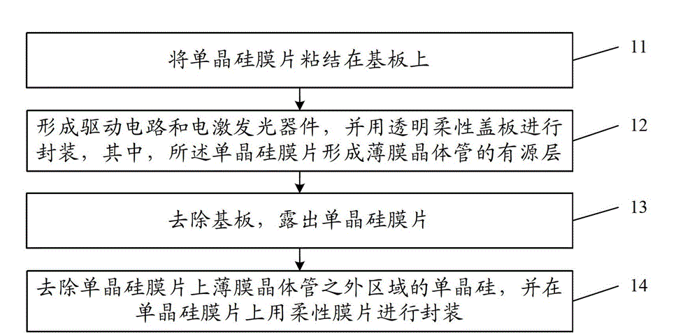
[0087] An embodiment of the present invention provides a method for manufacturing a flexible display device, such as figure 2 As shown, the method includes:

[0088] Step 11, bonding the monocrystalline silicon diaphragm 200 on the substrate 201, such as image 3 , 4 shown;

[0089] Compared with polycrystalline silicon, single crystal silicon has higher electron mobility and very uniform electrical conductivity, and can produce excellent p-type silicon semiconductors and n-type silicon semiconductors. The method of making single crystal silicon is usually to make polycrystalline silicon or amorphous silicon first, and then grow rod-shaped single crystal silicon from the melt by Czochralski method or suspension zone melting method. After the single crystal silicon rod is polished and sliced, it becomes Single crystal silicon wafer, the single crystal silicon diaphragm in this step can be cut from the single crystal silicon wafer according to the size of the display screen ...

specific Embodiment approach

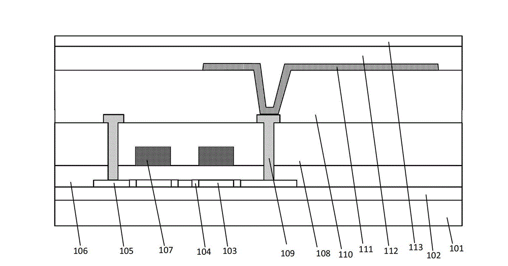
[0093] In this step, a thin film transistor and an electroluminescent device are formed, and an optional specific implementation is as follows:

[0094] 121. If Figure 5 As shown, a gate insulating layer 206 is formed on the single crystal silicon diaphragm 200;

[0095] Optionally, a gate insulating layer 206 is deposited on the monocrystalline silicon diaphragm 200 by plasma chemical vapor deposition (PECVD), and the gate insulating layer 206 can be a silicon nitride SiNx film layer, or a silicon oxide SiOx film layer, or Composite film layer of the two.

[0096] 122. If Figure 6 As shown, a gate electrode layer is formed on the gate insulating layer 206, and a gate electrode 207 is formed by a patterning process;

[0097] In this step, a gate electrode layer is deposited on the gate insulating layer 206 , and the gate electrode 207 can be formed through glue coating, exposure, development, and etching processes.

[0098] 123. Perform doping, and the single crystal sil...

Embodiment 2

[0128] The present invention also provides a flexible display device, which can be used in any products or components with display functions such as electronic paper, mobile phones, tablet computers, televisions, monitors, notebook computers, digital photo frames, navigators, etc., such as Figure 13 As shown, the device includes:

[0129] flexible diaphragm 214;

[0130] The driving circuit and the electroluminescent device arranged on the flexible diaphragm 214, wherein the active layer of the thin film transistor in the driving circuit is formed by the same single crystal silicon diaphragm, and the thin film transistor includes a first thin film transistor in the display area;

[0131] The transparent flexible cover plate 213 is packaged on the electroluminescence device.

[0132] Compared with the existing technologies, the flexible display device provided by the embodiments of the present invention has the advantages of being bendable, having higher resolution and more ...


PUM


Abstract

The invention discloses a flexible display device and a manufacturing method thereof and relates to the field of display. The manufacturing method is simple and can realize flexible display. In addition, the high-quality display picture can be obtained without a threshold voltage compensation circuit and an external driving integrated circuit. The method comprises the following steps: bonding a monocrystalline silicon diaphragm on a substrate, forming a driving circuit and an electroluminescence device on the substrate bonded with the monocrystalline silicon diaphragm, and packaging on the electroluminescence device with a transparent flexible cover plate, wherein the monocrystalline silicon diaphragm forms an active layer of a thin film transistor in the driving circuit; the thin film transistor comprises a first thin film transistor arranged in the display area of the flexible display device; the monocrystalline silicon outside the thin film transistor is removed from the monocrystalline silicon diaphragm; and the monocrystalline silicon diaphragm is sealed with the flexible diaphragm. The invention further provides a flexible display device manufactured by the method. Compared with the existing device, the flexible display device has the advantages of uniform brightness, simple structure and higher resolution.

Description

technical field [0001] The invention relates to the display field, in particular to a flexible display device and a manufacturing method thereof. Background technique [0002] Flexible display refers to a variable and bendable display device, generally using Active Matrix Organic Light Emitting Diode (AMOLED) or Polymer Light-emitting Diode (PLED) technology, which has low power consumption, Directly visible, variable and bendable, light and thin, impact resistant and not easy to damage, can be installed on curved surfaces, and made into wearable displays. It is expected to become the mainstream in the display field in the next few years. [0003] The AMOLED display is usually composed of a low temperature polysilicon (Low Temperature Poly-Silicon, LTPS) driven backplane and an electro-luminescence (Electro-Luminescence, EL) layer to form a self-luminous component. The structure of the traditional LTPS type AMOLED display is as follows figure 1 As shown, the preparation pr...

Claims


Application Information

Patent Timeline
Patent Type & Authority Applications(China)
IPC IPC(8): H01L27/32H01L21/77
Inventor 杨玉清李炳天朴承翊曹成熙
Owner BOE TECH GRP CO LTD
Why Eureka
Try Eureka