Source-drain buried graphene transistor device on diamond-like carbon substrate and manufacture method

A diamond and graphene technology, used in semiconductor/solid-state device manufacturing, semiconductor devices, electrical components, etc., can solve the problem of reducing graphene carrier mobility, reducing parasitic capacitance and channel resistance, and restricting device high-frequency performance. and size and other issues, to achieve the effect of small horizontal spacing, small channel resistance, and small parasitic capacitance

Inactive Publication Date: 2013-03-27
INST OF MICROELECTRONICS CHINESE ACAD OF SCI
View PDF2 Cites 17 Cited by
  • Summary
  • Abstract
  • Description
  • Claims
  • Application Information

AI Technical Summary

Problems solved by technology

[0003] At present, the main technical difficulties faced by graphene transistors are: 1) Graphene is a zero-bandgap material, how to obtain a certain bandgap by doping or applying external bias, or introducing stress, etc.
2) The interface between graphene and traditional silicon dioxide insulation has relatively strong phonon scattering, which seriously reduces the carrier mobility of graphene. How to grow high-quality insulation with less trap charges, fewer dangling bonds, and weak phonon scattering The upper and lower interfaces are an important issue to improve the performance of graphene transistors
3) The contact resistance between graphene and metal, and the graphene resistance not covered by the gate electrode between the source-drain region and the gate restrict the high-frequency performance and size reduction of the device
Therefore, the graphene transistors of the prior art cannot reduce the parasitic capacitance and the channel resistance at the same time.

Method used


Image

  • Source-drain buried graphene transistor device on diamond-like carbon substrate and manufacture method
  • Source-drain buried graphene transistor device on diamond-like carbon substrate and manufacture method
  • Source-drain buried graphene transistor device on diamond-like carbon substrate and manufacture method

Examples


Embodiment Construction

[0028] The present invention will be described in detail below in conjunction with the accompanying drawings and by taking specific implementations as examples. However, those skilled in the art should know that the present invention is not limited to the specific embodiments listed, as long as it conforms to the spirit of the present invention, it should be included in the protection scope of the present invention.

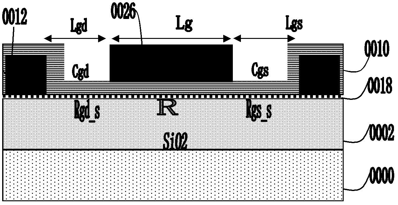
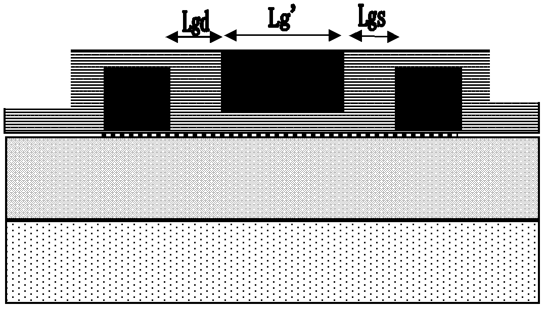
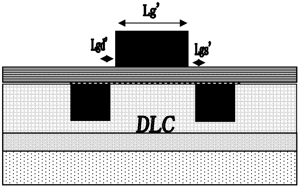
[0029] Basic principle of the present invention is as follows: diamond-like amorphous carbon (Diamond-like amorphous Carbon, abbreviated as DLC) thin film is a kind of very flat surface rich in Sp The amorphous carbon existence form of composition (reference: Michael Moseler.et al. The Ultrasmoothness of Diamond-like Carbon Surfaces. Science 3091545 (2005)). Diamond-like amorphous carbon has stable chemical properties, less surface trap charges and dangling bonds, and can form a weaker п bond with the graphene interface, which can obtain a better quality interfac...


PUM

PropertyMeasurementUnit
thicknessaaaaaaaaaa
compressive stressaaaaaaaaaa
thicknessaaaaaaaaaa

Abstract

A source-drain buried graphene transistor device on a diamond-like carbon substrate and a manufacture method are applicable to radio frequency communication. The manufacture method includes: firstly, depositing a layer of diamond-like carbon amorphous carbon smooth in surface and stable in chemical property on the substrate by the aid of a magnetic filtered cathode vacuum arc system; secondly, etching a source trench and a drain trench on the diamond-like carbon amorphous carbon insulating layer and filling electrode metal into the trenches; thirdly, planarizing and cleaning the surface of the substrate prior to transferring graphene grown by a chemical vapor deposition method to the cleaned substrate; fourthly, growing gate insulating dielectric by an atomic layer deposition method and sputtering gate electrode metal; and finally, forming a metal gate by means of reactive ion etching and depositing low-K insulating dielectric to protect the device. Carrier mobility of a graphene transistor is high, and the source-drain buried structure is capable of decreasing the graphene length of a region uncovered by the gate, so that gate-source capacitance, gate-drain capacitance and channel resistance are reduced, and high-frequency performance and efficiency of the graphene transistor are improved. The source-drain buried graphene transistor device can be widely applied to small-sized high-frequency graphene integrated circuits.

Description

technical field [0001] The invention relates to the technical field of semiconductors, in particular to a source-drain buried type graphene transistor device and a manufacturing method on a diamond-like substrate suitable for radio frequency communication. Background technique [0002] Since Novoselov et al. reported about the successful preparation of one-way graphene and discovered the electric field effect in graphene in 2004, graphene has been widely concerned and researched (reference: Electric Field Effect in Atomically Thin Carbon Films K.S.Novoselov.et al . Science 22 October 2004: 306(5696), 666-669.). Graphene is favored by semiconductor device engineers for its very high mobility and unit layer thickness. Especially in high-frequency applications, graphene has shown great potential. Various research groups around the world are vying to report the high-frequency performance of graphene, and the cut-off frequency of graphene transistors has reached 100G-300G. In t...

Claims


Application Information

Patent Timeline
Patent Type & Authority Applications(China)
IPC IPC(8): H01L29/08H01L29/16H01L29/78H01L21/762H01L21/336
Inventor 马小龙殷华湘
Owner INST OF MICROELECTRONICS CHINESE ACAD OF SCI
Why Eureka
Try Eureka