Heterojunction bipolar transistor with electrode shielding structure and manufacturing method thereof
A heterojunction bipolar, shielding structure technology, used in semiconductor/solid-state device manufacturing, circuits, electrical components, etc., can solve the problem of high frequency performance impact, etc., to improve device performance, improve circuit speed, reduce The effect of transmission delay
- Summary
- Abstract
- Description
- Claims
- Application Information
AI Technical Summary
Problems solved by technology
Method used
Image
Examples
Embodiment 1
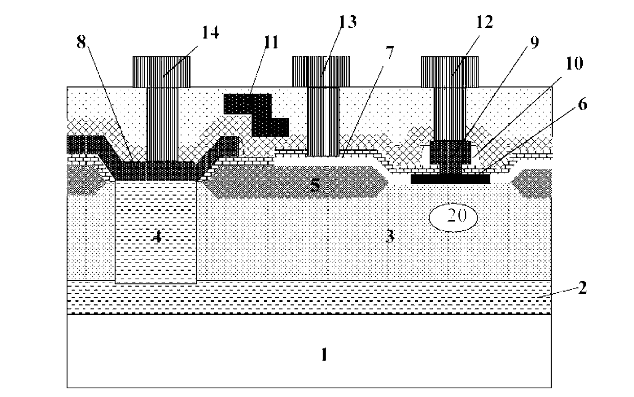
[0026] Preferred embodiment one: as figure 1 As shown, to prepare a bipolar transistor with a common emitter connection method, first prepare a heavily doped P-type substrate silicon wafer 1 . After growing the thin oxide layer, N+ impurities are implanted by photolithography, and then the buried layer 2 is formed. After etching the oxide layer, an N-epitaxial layer 3 is grown.
[0027] Photolithography, implanting N+ impurities to form the lead-out part 4 from the buried layer to the collector. An oxide layer is grown, silicon nitride is deposited, and then the oxide layer and silicon nitride are etched by photolithography to form a field oxygen window, and a thick oxide layer is grown as the field oxide layer 5, and then silicon nitride is removed.
[0028] Lithograph the SIC window, inject N-type impurities, and anneal to form the SIC20; then deposit polysilicon, and then photoetch and etch the polysilicon to form a silicon-germanium epitaxial window, and make a silicon-g...
Embodiment 2
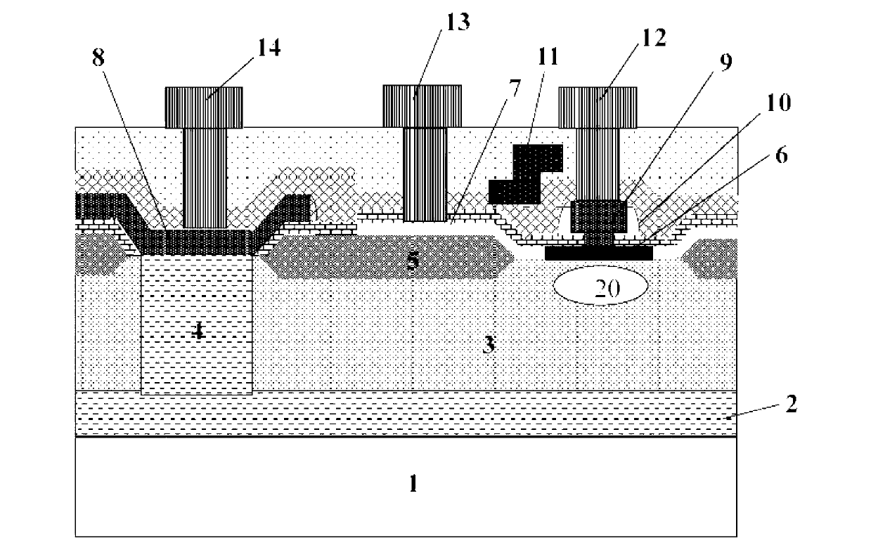
[0032] Preferred embodiment two: as figure 2 As shown, to prepare a bipolar transistor with a common collector connection method, first prepare a heavily doped P-type substrate silicon wafer 1 . After growing the thin oxide layer, N+ impurities are implanted by photolithography, and then the buried layer 2 is formed. After etching the oxide layer, an N-epitaxial layer 3 is grown.
[0033] Photolithography, implanting N+ impurities to form the lead-out part 4 from the buried layer to the collector. An oxide layer is grown, silicon nitride is deposited, and then the oxide layer and silicon nitride are etched by photolithography to form a field oxygen window, and a thick oxide layer is grown as the field oxide layer 5, and then silicon nitride is removed.
[0034] Lithograph the SIC window, inject N-type impurities, and anneal to form the SIC20; then deposit polysilicon, and then photoetch and etch the polysilicon to form a silicon-germanium epitaxial window, and make a silico...
PUM
 Abstract
Description
Claims
Application Information
 - R&D Engineer
- R&D Manager
- IP Professional
- Industry Leading Data Capabilities
- Powerful AI technology
- Patent DNA Extraction
Browse by: Latest US Patents, China's latest patents, Technical Efficacy Thesaurus, Application Domain, Technology Topic, Popular Technical Reports.
© 2024 PatSnap. All rights reserved.Legal|Privacy policy|Modern Slavery Act Transparency Statement|Sitemap|About US| Contact US: help@patsnap.com


