Solar battery with band gap gradual changing silicon quantum dot multilayer film and production method thereof

A technology of silicon quantum dots and solar cells, applied in circuits, photovoltaic power generation, electrical components, etc., can solve problems such as the decline of collection efficiency and conversion efficiency, unfavorable tunnel operation of transmission channels, and increasing the number of battery interface layers, and achieve good battery response. and energy conversion efficiency, expand the wavelength range of light response, and facilitate mass production.

Inactive Publication Date: 2013-03-27
NANJING UNIV
View PDF1 Cites 17 Cited by
  • Summary
  • Abstract
  • Description
  • Claims
  • Application Information

AI Technical Summary

Problems solved by technology

However, in order to realize this stacked solar cell structure, it is necessary to use silicon nanomaterials of different sizes to form sub-cells, which not only increases the difficulty of the process, but also needs to use heavily doped semiconductor layers to form tunnel junctions between the sub-cells, increasing the battery life. The number of interface layers will cause the recombination loss of carriers on the interface. Another important problem is that the current matching between each sub-cell is difficult to achieve, which greatly limits the efficiency of silicon quantum dot stacked cells.
[0007] Technically speaking, although the nano-Si structure is an important way to realize the effective absorption of short-wavelength light, the current preparation method of nano-silicon materials is generally to form a mosaic-type nano-silicon film from silicon-rich silicon oxide by high-temperature annealing. For the sub-cells composed of nano-silicon, it is necessary to prepare silicon-rich silicon oxide films with different composition ratios to form sub-cells, so that it is difficult for the photo-generated carriers generated in nano-Si to pass through the insulating SiO 2 transported to the electrodes on both sides to form a photocurrent
On the other hand, there are too many interfaces, and the interface states act as recombination centers or traps, which reduces the photogenerated current passing through the junction. Furthermore, the size and distribution of nano-silicon grains are random, which is not conducive to the tunneling operation of the transmission channel, and eventually leads to open circuit voltage. decrease (the measured open circuit voltage is only 463mV) [7], the collection efficiency and conversion efficiency decrease

Method used


Image

  • Solar battery with band gap gradual changing silicon quantum dot multilayer film and production method thereof
  • Solar battery with band gap gradual changing silicon quantum dot multilayer film and production method thereof
  • Solar battery with band gap gradual changing silicon quantum dot multilayer film and production method thereof

Examples


Embodiment Construction

[0047] The general steps that the present invention prepares:

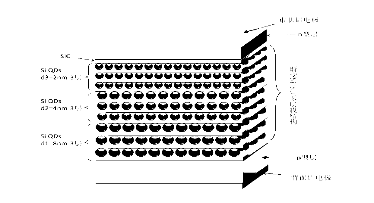
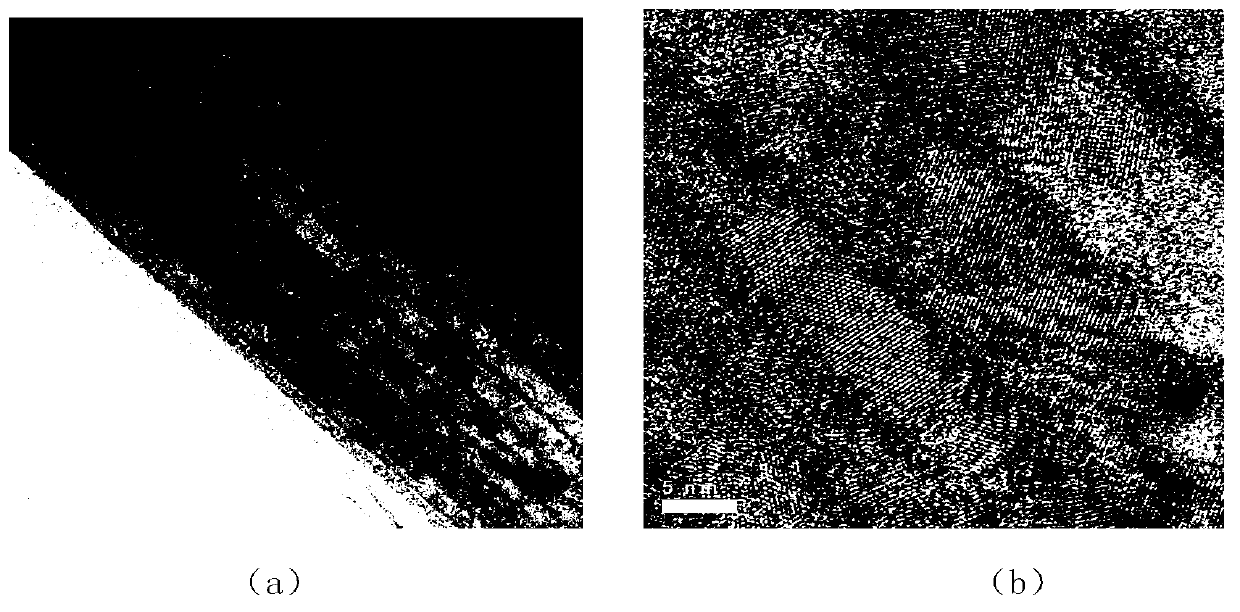
[0048] The first step: preparing an amorphous silicon / silicon carbide multilayer film structure with a gradual thickness on a p-type silicon substrate;

[0049] 1-1. Growth by chemical vapor deposition or plasma enhanced chemical vapor deposition in a chemical vapor deposition or plasma enhanced chemical vapor deposition system, the substrate temperature is controlled at 250°C, the radio frequency power can be varied between 30W and 50W, and silane is used (SiH 4 ) and methane (CH 4) mixed gas as a reaction gas source, and a hydrogenated amorphous silicon carbide film with a certain thickness is deposited on a p-type single crystal silicon substrate;

[0050] 1-2. After the deposition of the hydrogenated amorphous silicon carbide film is completed, the methane gas source is turned off, and only silane gas is introduced to prepare the hydrogenated amorphous silicon film;

[0051] 1-3. The above two processes are...


PUM

PropertyMeasurementUnit
thicknessaaaaaaaaaa

Abstract

A solar battery with a band gap gradual changing silicon quantum dot multilayer film comprises a p type silicon substrate, wherein a thickness gradual changing multilayer amorphous silicon / silicon carbide film structure, a thickness gradual changing amorphous silicon / silicon carbide grease silicon quantum dot / silicon carbide multilayer film structure and a p-i-n battery structure are arranged on the p type silicon substrate, the p-i-n battery structure is formed by the p type silicon substrate, a silicon carbide intrinsic layer (namely an i layer) and the outermost n type nanocrystalline silicon film, and an electrode is guided out on the surface of the p type silicon substrate to form a battery. The thickness of amorphous silicon sub layers in the period of each hydrogenation amorphous silicon / silicon carbide growing towards the surface of the p type silicon substrate is thinned gradually. The amorphous silicon sub layer growing on the p type silicon substrate or close to the p type silicon substrate is the thickest, and the amorphous silicon sub layer growing towards the surface of the p type silicon substrate is the thinnest.

Description

1. Technical field: [0001] The invention belongs to the field of new energy materials and new solar cell devices. In particular, it relates to a solar cell based on a multilayer film structure of silicon quantum dots with a graded band gap and its preparation. 2. Background technology: [0002] Silicon is the material of choice for large-scale application of solar cells, but its band gap is 1.1eV, the near-infrared and near-ultraviolet photon energy in sunlight cannot be fully absorbed and utilized, and the effective response spectrum is only in the range of 500-900nm, so there is a so-called The Shockley-Queisser limit of single-junction silicon solar cell efficiency. In response to this problem, in order to solve the key problem of obtaining high-efficiency Si-based solar cells, the present invention utilizes the preparation of amorphous silicon films / silicon carbide multilayer films with different thicknesses, and through post-processing (thermal annealing or laser annea...

Claims


Application Information

Patent Timeline
Patent Type & Authority Applications(China)
IPC IPC(8): H01L31/075H01L31/0352H01L31/20
CPCY02E10/50Y02E10/548Y02P70/50
Inventor 徐骏曹蕴清绪欣李淑鑫芮云军李伟徐岭陈坤基孙胜华张晓伟陆鹏许杰
Owner NANJING UNIV
Why Eureka
Try Eureka