Silicon carbide (SIC) transverse Schottky junction type mini-sized nuclear battery and manufacturing method thereof

A Schottky junction and silicon carbide technology, which is used in nuclear engineering, obtaining electrical energy from radioactive sources, and applications of radiation from radioactive sources. and other problems, to achieve the effect of improving fill factor, improving energy conversion efficiency, and flexible design

Inactive Publication Date: 2013-04-10
CHANGAN UNIV
View PDF9 Cites 2 Cited by
  • Summary
  • Abstract
  • Description
  • Claims
  • Application Information

AI Technical Summary

Problems solved by technology

As a result, incident particles must traverse the Schottky metal electrode, causing significant loss of particle energy
Although it has been proposed to use translucent electrodes and other methods to solve this problem, that structure also poses difficulties to the process and application.
[0008] 2. The problem of vertical structure
However, the vertical structure will increase the series resistance of the device, resulting in a decrease in the fill factor and a reduction in the maximum output power of the battery.
At the same time, the vertical structure is not conducive to integration and is not conducive to improving packaging density

Method used


Image

  • Silicon carbide (SIC) transverse Schottky junction type mini-sized nuclear battery and manufacturing method thereof
  • Silicon carbide (SIC) transverse Schottky junction type mini-sized nuclear battery and manufacturing method thereof
  • Silicon carbide (SIC) transverse Schottky junction type mini-sized nuclear battery and manufacturing method thereof

Examples


Embodiment 1

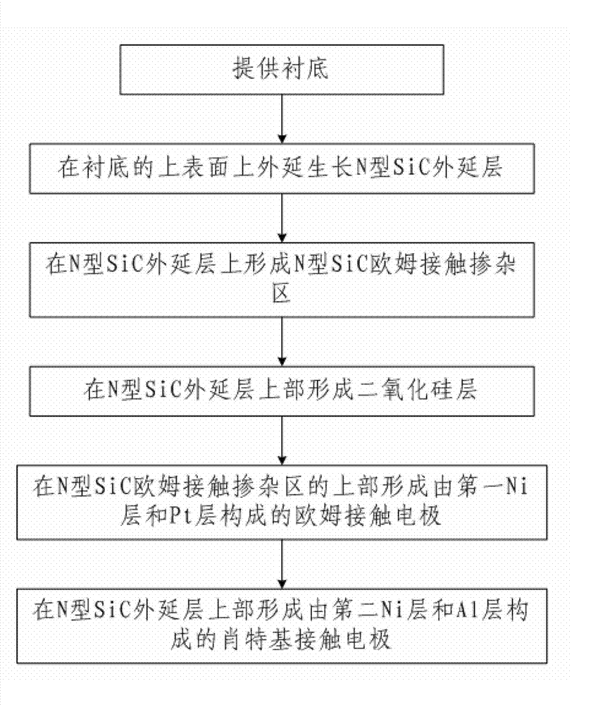
[0050] combine image 3 A method for manufacturing a silicon carbide lateral Schottky junction micro-nuclear battery according to the present invention, comprising the following steps:

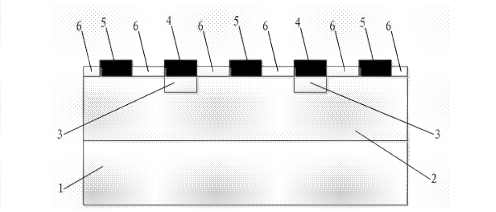
[0051] Step 1: Provide a substrate 1, which is composed of an N-type SiC substrate; when step 1 is completed, the schematic diagram of the structure of a silicon carbide lateral Schottky junction micro-nuclear battery is as follows Figure 4a shown;

[0052] Step 2. Epitaxially grow on the upper surface of the substrate 1 with a doping concentration of 1×10 by using a low pressure hot wall chemical vapor deposition method. 15 cm -3 , N-type SiC epitaxial layer 2 with a thickness of 5 μm, the epitaxial growth temperature is 1570 ° C, the epitaxial growth pressure is 100 mbar, and the epitaxial growth gas is C with a volume ratio of 2:1:4 3 h 8 、SiH 4 and H 2 The mixed gas; the structure schematic diagram of silicon carbide lateral Schottky junction micro-nuclear battery when step 2 is com...

Embodiment 2

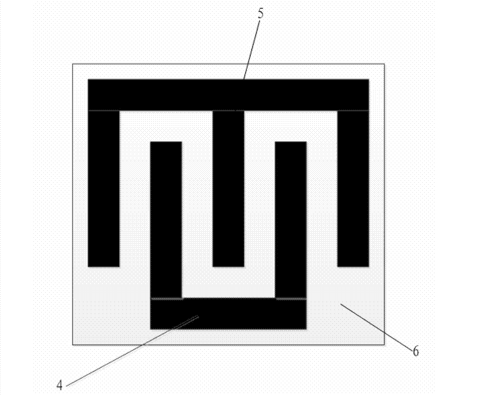
[0059] The difference between this embodiment and Embodiment 1 is that in step 2, the epitaxial growth on the upper surface of the substrate 1 with a doping concentration of 3×10 15 cm -3 , an N-type SiC epitaxial layer 2 with a thickness of 6.5 μm; in step 3, an ion implantation method is used to form a doping concentration of 3×10 on the N-type SiC epitaxial layer 2 18 cm -3 The N-type SiC ohmic contact doped region 3, and thermal annealing at a temperature of 1565° C. for 10 minutes in an Ar atmosphere; in step 4, the N-type SiC epitaxial layer 2 is formed by dry oxygen oxidation at a temperature of 1150° C. The upper part is formed with a thickness of 15nm silicon dioxide layer 6; in step 5, electron beams are used to evaporate metal Ni and Pt successively in the first finger window, and 2 Perform thermal annealing at a temperature of 965° C. for 2 minutes in an atmosphere, and form an ohmic contact electrode 4 composed of a first Ni layer and a Pt layer on the upper par...

Embodiment 3

[0062] The difference between this embodiment and Embodiment 1 is that in step 2, the epitaxial growth on the upper surface of the substrate 1 with a doping concentration of 5×10 15 cm -3 , an N-type SiC epitaxial layer 2 with a thickness of 8.5 μm; in step 3, an ion implantation method is used to form a doping concentration of 5×10 on the N-type SiC epitaxial layer 2 18 cm -3 The N-type SiC ohmic contact doped region 3, and thermal annealing at a temperature of 1580° C. for 10 minutes in an Ar atmosphere; in step 4, the N-type SiC epitaxial layer 2 is formed by dry oxygen oxidation at a temperature of 1150° C. The upper part is formed with a thickness of 20nm silicon dioxide layer 6; in step 5, electron beams are used to evaporate metal Ni and Pt successively in the first finger window, and 2 Perform thermal annealing at a temperature of 985° C. for 2 minutes in an atmosphere, and form an ohmic contact electrode 4 composed of a first Ni layer and a Pt layer on the upper par...


PUM

PropertyMeasurementUnit
thicknessaaaaaaaaaa
thicknessaaaaaaaaaa
thicknessaaaaaaaaaa

Abstract

The invention discloses a silicon carbide (SIC) transverse Schottky junction type mini-sized nuclear battery and a manufacturing method thereof. The nuclear battery comprises a substrate and an N type SIC outer epitaxial layer arranged on the upper portion of the substrate. The N type SIC outer epitaxial layer is provided with an N type SIC ohmic contact doped region. An ohmic contact electrode is arranged on the upper portion of N type SIC ohmic contact doped region. The upper portion of the N type SIC outer epitaxial layer is provided with a Schottky contact electrode. A silicon dioxide layer is arranged on the upper portion, except the areas of the ohmic contact electrode and the Schottky contact electrode, of the N type SIC outer epitaxial layer. The manufacturing method of the nuclear battery comprises the steps of providing the substrate; forming the N type SIC outer epitaxial layer on the substrate in an epitaxial growth mode; forming the N type SIC ohmic contact doped region; forming the silicon dioxide layer; forming the ohmic contact electrode; and forming the Schottky contact electrode; The SIC transverse Schottky junction type mini-sized nuclear battery is reasonable in design, favorable to improving energy converting efficiency and packaging density of mini-sized nuclear batteries, favorable to integration, strong in practicality, and high in popularization and utilization value.

Description

technical field [0001] The invention relates to the technical field of semiconductor devices and semiconductor processes, in particular to a silicon carbide lateral Schottky junction micro-nuclear battery and a manufacturing method thereof. Background technique [0002] A micronuclear battery is a device that uses semiconductor diodes as an energy conversion structure to directly convert nuclear energy into electrical energy. It uses radioactive isotopes (such as 63 Ni, 147 The ionization effect of the radiation particles emitted by Pm) in the semiconductor material is used as an energy source, and the electron-hole pairs generated by the radiation particles in the semiconductor are collected to generate output power. [0003] The maximum output power of the micro-nuclear battery is: P out =FF·V OC I SC . where FF is the fill factor, V OC is the open circuit voltage, I SC is the short circuit current. [0004] Under the determined irradiation source and device area,...

Claims


Application Information

Patent Timeline
Patent Type & Authority Applications(China)
IPC IPC(8): G21H1/06
Inventor 张林李清华邱彦章巨永锋
Owner CHANGAN UNIV
Why Eureka
Try Eureka