Photoetching method and system using metal glass as photoresist

A metal glass and photolithography system technology, applied in the field of micro-nano device manufacturing, can solve the problems of high price, limitation, and the edge of the groove is not steep enough, and achieve the effect of high output rate, high cost performance, and loose operating environment requirements.

Active Publication Date: 2013-04-17
HUAZHONG UNIV OF SCI & TECH
View PDF5 Cites 7 Cited by
  • Summary
  • Abstract
  • Description
  • Claims
  • Application Information

AI Technical Summary

Problems solved by technology

However, since the phase change lithography selectivity of the chalcogenide semiconductor phase change material itself (the ratio of the etching rate of the two phases in the solution) is only about 2, and this series of materials and their multilayer films are used to produce phase change lithography The edge of the groove is not steep enough and the price is relatively expensive, so the application of this method is limited in a certain period of time

Method used


Image

  • Photoetching method and system using metal glass as photoresist
  • Photoetching method and system using metal glass as photoresist
  • Photoetching method and system using metal glass as photoresist

Examples


Embodiment 1

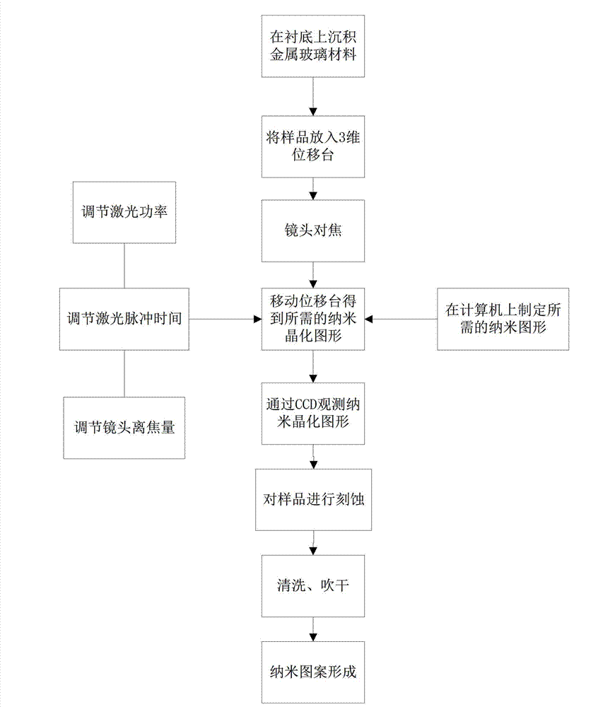
[0058] MgCuY metallic glass material was prepared on a quartz substrate by magnetron sputtering method, the sputtering parameters were: power 60W, Ar pressure 0.5Pa, sputtering time 20min, target base distance 100mm;

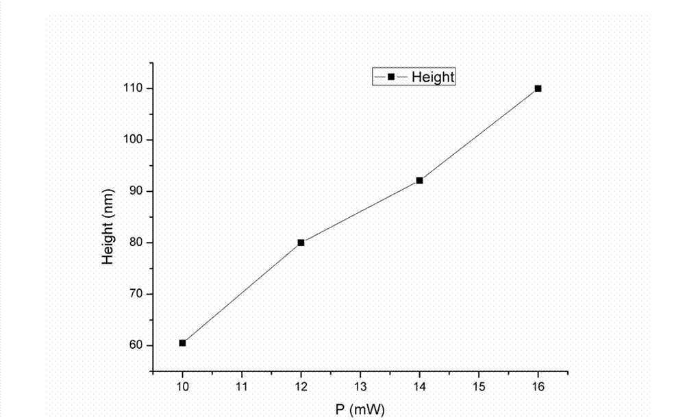
[0059] Photolithography of MgCuY metallic glass material, using Corrent-660-100-C semiconductor laser, Japan Sigma focusing lens (NA=0.4), the minimum crystallization point diameter obtained after photolithography is 600nm, which is much smaller than the spot diffraction of this lens The limit is 2.013um; expose the sample, the exposure power is 10mW, 12mW, 14mW, 16mW, and the moving rate of the three-dimensional translation stage is 100um / s; put the exposed sample into 3%HNO 3 solution for 60s, the obtained step height is as follows image 3 Shown:

[0060] It can be seen from the figure that as the laser power increases, the crystallization degree of the MgCuY metallic glass sample increases, and the step height after etching increases with the increase of la...

Embodiment 2

[0062] Exposure steps:

[0063] Using Corrent-660-100-C semiconductor laser, Japan Sigma focusing lens (NA=0.4), using magnetron sputtering method to prepare ZnS-SiO on the substrate 2 , AlNiGd, ZnS-SiO 2 The 3-layer thin film can control the lithographic crystallization line width by controlling the laser pulse time, power, and lens defocus degree;

[0064] Figure 4 is the relationship between the laser pulse time and the lithographic linewidth of the multilayer metallic glass sample; it can be seen from the figure that under the same laser power condition, the crystallization linewidth of the above three-layer film sample increases with the increase of the laser pulse time, When the pulse time is 180ns, the crystallization linewidth is 1.41um; when the pulse time is 80ns, the crystallization linewidth is 0.52um; the crystallization linewidth can be changed in a small size range by simply changing the laser pulse time; and It can be seen that at 80ns, the lithographic lin...


PUM


Abstract

The invention discloses a photoetching method using a metal glass as a photoresist. The method specifically comprises the following steps: depositing a metal glass material photoresist layer on the surface of a substrate; exposing a sample obtained through depositing according to a target nanometer pattern; generating a nanometer crystallized graphic at an exposed part when the exposed part reaching the crystallization temperature is changed in phase; and etching the exposed sample with the nanometer crystallized graphic so as to form a desired nanometer pattern. According to the invention, as the metal glass material replaces an organic photoresist, the photoetching line width of the obtained sample can be far smaller than the diffraction limit of a laser focusing spot; and moreover, low cost and large etching selection ratio are obtained. The invention further discloses a system for realizing the method; and the system mainly comprises a computer, an arbitrary waveform generator, a semiconductor laser, a collimating beam expander, a beam isolator, a beam splitter, a focusing servo mechanism, a focusing lens, an X-Y-Theta three-dimensional displacement platform and a focusing servo control box. The system disclosed by the invention has the advantages of simple composition, high performance cost, simplicity in operation, comparatively low requirement on operation environment and high output rate.

Description

technical field [0001] The invention belongs to the field of micro-nano device manufacturing, and specifically relates to a photolithography method using metallic glass as a photoresist, a phase-change photolithography system for performing photolithography on metallic glass, and detection of phase-change degree of phase-change materials in the system detection parts. Background technique [0002] In the current manufacturing process of semiconductor devices, optical disc masters, sensors, optoelectronic devices, micro-electromechanical system devices, etc., there is no doubt that there is a step of preparing nano-apertures. Up to now, the method of preparing nano-apertures is mainly There are three types: [0003] (1) Electron beam lithography (EBL); [0004] (2) Focused ion beam lithography (FIBL); [0005] (3) Photolithography (PL); [0006] Since electron beam lithography (EBL) and focused ion beam lithography (FIBL) require strict vacuum conditions, lithography equi...

Claims


Application Information

Patent Timeline
Patent Type & Authority Applications(China)
IPC IPC(8): G03F7/20
Inventor 缪向水曾笔鉴李震黄君竹
Owner HUAZHONG UNIV OF SCI & TECH
Why Eureka
Try Eureka