Fe-Cr-Si ternary amorphous thin film capable of modulating band gap width and preparation method thereof

A fe-cr-si, amorphous thin film technology, applied in the field of Fe-Cr-Si ternary amorphous thin film and its preparation, can solve the problem of multiphase hybrid deterioration, prone to stacking fault, twinning, large film base loss. Matching and other problems, to achieve the effect that the process conditions are easy to control, the application prospect is broad, and the industrialization is convenient.

Inactive Publication Date: 2014-12-10
DALIAN UNIV OF TECH
View PDF1 Cites 0 Cited by
  • Summary
  • Abstract
  • Description
  • Claims
  • Application Information

AI Technical Summary

Problems solved by technology

The crystals are also prone to defects such as stacking faults and twins, so it is difficult to obtain high-quality and pure β-FeSi 2 Material
[0005] (2) β-FeSi 2 When used in the field of optoelectronics, most of the thin films are prepared on the basis of single crystal Si, but there is a large film-base mismatch problem, resulting in many of its properties failing to meet theoretical expectations.
[0006] (3) Binary β-FeSi currently prepared using different methods 2 material, whose bandgap width varies around 0.87eV, is slightly different, but cannot be modulated
Crystalline ternary FeSi after adding the third component 2 Type materials are prone to phase separation. Although the bandgap width can be modulated in a wide range, it increases the instability of the structure and further deteriorates the situation of multiphase mixing.

Method used


Image

  • Fe-Cr-Si ternary amorphous thin film capable of modulating band gap width and preparation method thereof
  • Fe-Cr-Si ternary amorphous thin film capable of modulating band gap width and preparation method thereof
  • Fe-Cr-Si ternary amorphous thin film capable of modulating band gap width and preparation method thereof

Examples


Embodiment 1

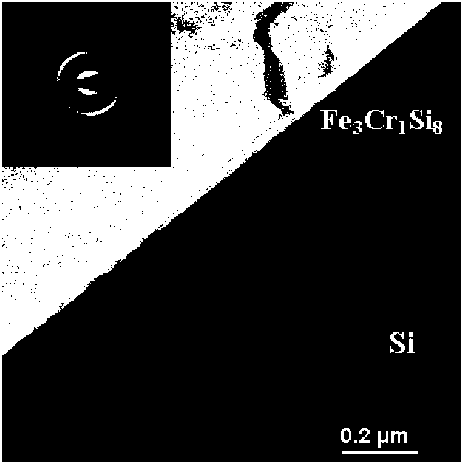
[0031] Embodiment 1: Fe is prepared by magnetron sputtering method 3 Cr 1 Si 8 film

[0032] (1) Preparation of alloy sputtering target, the steps are as follows:

[0033] ①Material preparation: Weigh the value of each component according to the atomic percentage of Fe and Cr at 3:1, and the purity of Fe and Cr metal raw materials to be used is above 99.9%;

[0034] ② Fe 3 Cr 1 Melting of alloy ingots: Put the metal mixture in the water-cooled copper crucible of the melting furnace, and use the method of vacuum arc melting to melt under the protection of argon. First, vacuumize to 10 -2 Pa, then filled with argon until the pressure is 0.03±0.01MPa, the control range of melting current density is 150±10A / cm 2 After melting, continue to smelt for 10 seconds, turn off the power, let the alloy cool down to room temperature with the copper crucible, then turn it over, put it back in the water-cooled copper crucible, and carry out the second smelting; the aforementioned proces...

Embodiment 2

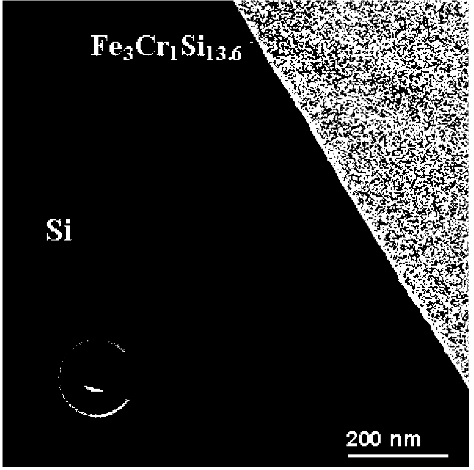
[0045] Embodiment 2: Fe is prepared by magnetron sputtering method 3 Cr 1 Si 13.6 film

[0046] The preparation process is the same as in Example 1, only the number of alloy sheets for preparing the combined alloy sputtering target is adjusted: by 5 sheets of Fe 3 Cr 1 The alloy sheet is pasted on the basic Si target used for sputtering. According to EPMA analysis, the contents of Fe, Cr, and Si in the film are 16.9 at.%, 5.7 at.%, and 77.4 at.%. The atomic ratio of Fe and Cr is 3:1, so the composition formula is written as Fe 3 Cr 1 Si 13.6 . The XRD and TEM results showed that the Fe 3 Cr 1 Si 13.6 No crystal information was found in the sample, indicating that the prepared amorphous film was prepared. TEM images measured the thickness of the film to be 315 nm, and the bandgap width was measured to be 0.54 eV.

Embodiment 3

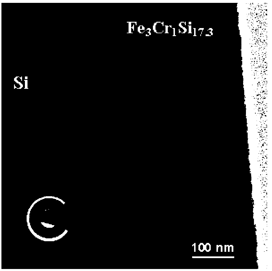
[0047] Embodiment 3: Fe is prepared by magnetron sputtering method 3 Cr 1 Si 17.3 film

[0048] The preparation process is the same as in Example 1, only the number of alloy sheets for preparing the combined alloy sputtering target is adjusted: by 4 sheets of Fe 3 Cr 1 The alloy sheet is pasted on the basic Si target used for sputtering. According to EPMA analysis, the contents of Fe, Cr, and Si in the film are 14.1 at.%, 4.7 at.%, and 81.2 at.%. The atomic ratio of Fe and Cr is 3:1, so the composition formula is written as Fe 3 Cr 1 Si 17.3 . The XRD and TEM results showed that the Fe 3 Cr 1 Si 17.3 No crystal information was found in the sample, indicating that the prepared amorphous film was prepared. The TEM image measured the thickness of the film to be 323 nm, and the bandgap width was measured to be 0.60 eV.


PUM

PropertyMeasurementUnit
diameteraaaaaaaaaa
thicknessaaaaaaaaaa
diameteraaaaaaaaaa

Abstract

The invention discloses a Fe-Cr-Si ternary amorphous thin film capable of modulating band gap width and a preparation method thereof, and belongs to the technical field of semiconductor materials. The Fe-Cr-Si ternary amorphous thin film has the following general formula: Fe3Cr1Six, wherein x is 8-18; along with increase of x from 8 to 18, the band gap width increases from 0 eV to 0.65 eV; and the thin film structure is amorphous. Compared with an ordinary binary transition metal silicide thin film, the Fe-Cr-Si ternary amorphous thin film has the advantages as follows: 1, the Fe3Cr1Six thin film is a novel ternary semiconductor amorphous thin film and can modulate the band gap width within a relatively large range of 0-0.65 eV; and under the action of Cr, the band gap width can be affected and the amorphous forming capability of the thin film can be increased through addition of one element; 2, the proportion of Si in the Fe3Cr1Six thin film can be conveniently regulated only by changing the number of Fe3Cr1 alloys in a combined sputtering target, thus obtaining different band gap widths; and 3, the Fe3Cr1Six thin film is amorphous, so that the uniformity of components and the performance can be ensured, and lattice mismatch and multiphase mixing and other problems during preparation of a crystalline thin film are effectively avoided. Therefore, the Fe-Cr-Si ternary amorphous thin film is applicable to production of near infrared detectors and other semiconductor devices with narrow band gaps.

Description

technical field [0001] The invention relates to a Fe-Cr-Si ternary amorphous thin film capable of modulating the bandgap width and a preparation method thereof, belonging to the technical field of semiconductor materials. Background technique [0002] Semiconductor metal silicides are one of the materials used in solar cells. They have excellent compatibility with single crystal silicon technology, and have metal conductivity, high thermal stability, oxidation resistance and superior mechanical stability. At the same time, semiconductor Silicides have also won widespread attention due to their superior environmental friendliness, especially transition metal silicides. The typical one is β-FeSi 2 and CrSi 2 . β-FeSi 2 It has a direct band gap of 0.83~0.87eV, and has a large optical absorption coefficient for infrared wavelengths (α>10 -5 cm -1 ,1.0eV), the theoretical photoelectric conversion efficiency can reach 16~23%, which can be used to prepare high-efficiency s...

Claims


Application Information

Patent Timeline
Patent Type & Authority Patents(China)
IPC IPC(8): C22C45/00C23C14/14C23C14/35
Inventor 李晓娜郑月红董闯
Owner DALIAN UNIV OF TECH
Why Eureka
Try Eureka