Multifunctional exposure imaging method based on composite dielectric grating metal-oxide-semiconductor field-effect transistor (MOSFET) light-sensitive detector

A technology of photosensitive detectors and composite media, applied in radiation control devices, etc., can solve the problems of low sensitivity and resolution, and achieve the effect of expanding the application range

Active Publication Date: 2013-06-19
南京威派视半导体技术有限公司
View PDF5 Cites 10 Cited by
  • Summary
  • Abstract
  • Description
  • Claims
  • Application Information

AI Technical Summary

Problems solved by technology

However, each pixel of CMOS-APS is composed of multiple transistors and a photosensitive diode (including amplifier and A/D conversion circuit), so that

Method used


Image

  • Multifunctional exposure imaging method based on composite dielectric grating metal-oxide-semiconductor field-effect transistor (MOSFET) light-sensitive detector
  • Multifunctional exposure imaging method based on composite dielectric grating metal-oxide-semiconductor field-effect transistor (MOSFET) light-sensitive detector
  • Multifunctional exposure imaging method based on composite dielectric grating metal-oxide-semiconductor field-effect transistor (MOSFET) light-sensitive detector

Examples


Embodiment Construction

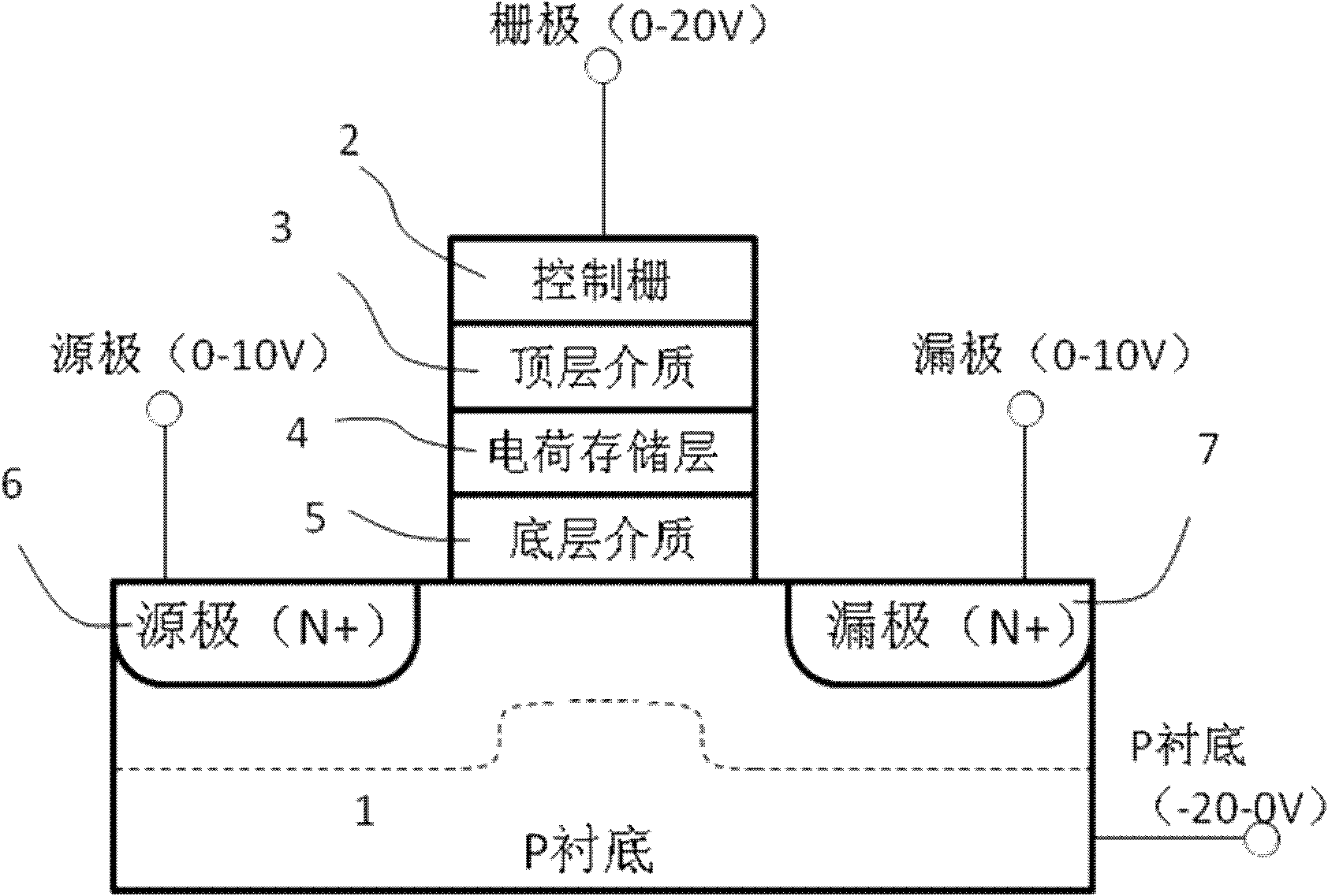
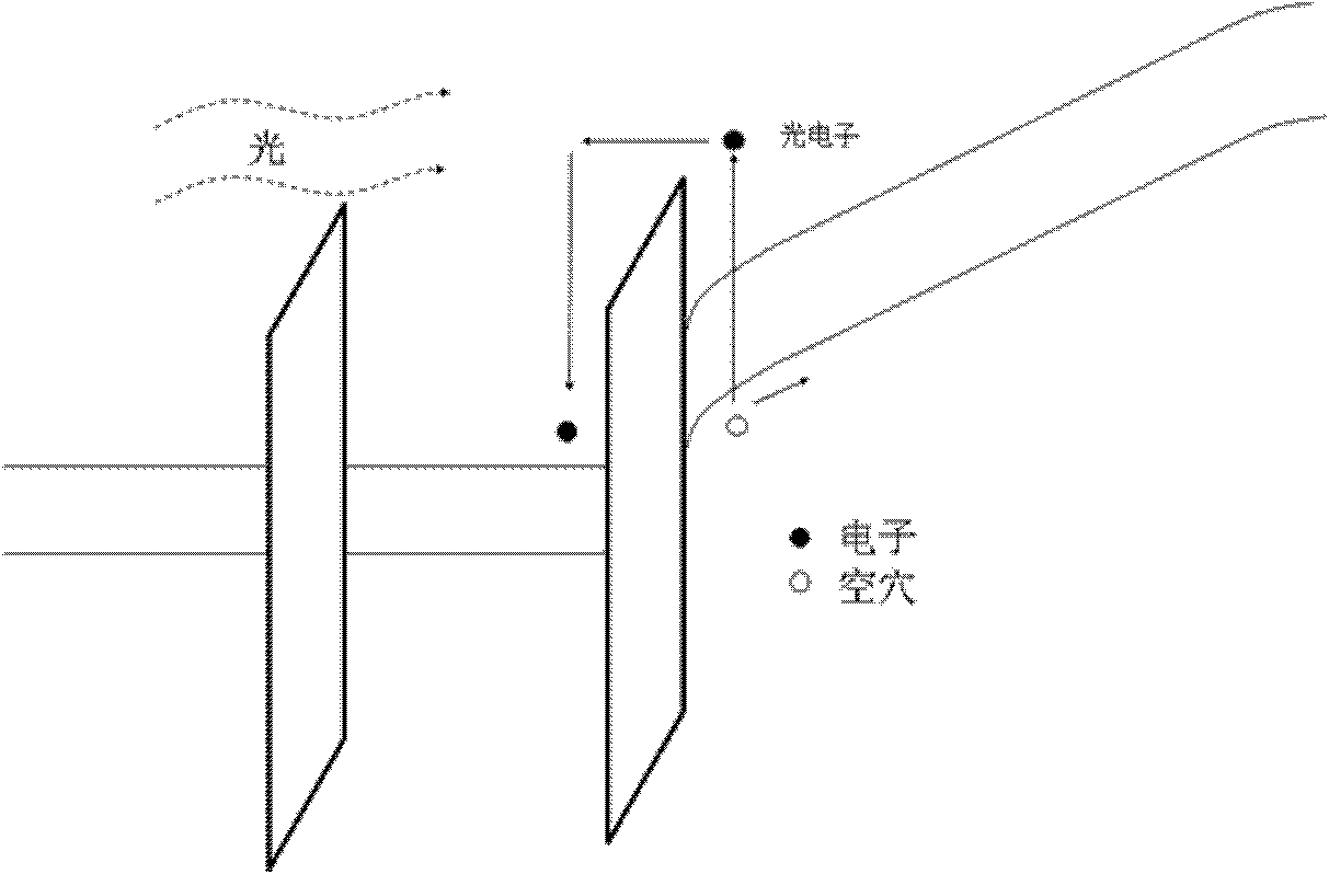
[0019] The working process and physical mechanism of the present invention will be described below with reference to the accompanying drawings as follows

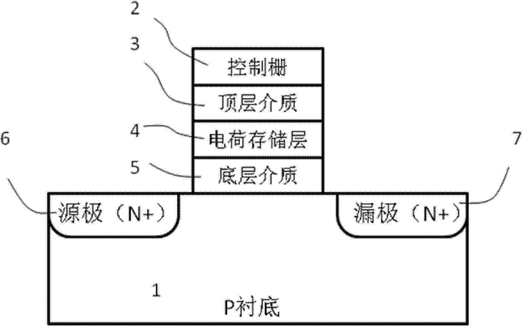
[0020] like figure 1 It is the basic structure of a composite dielectric gate MOSFET photosensitive detector, a semiconductor substrate (P type) 1, and a bottom insulating medium 5, an optoelectronic storage layer 4, a top insulating medium 3, a control gate 2, and a semiconductor substrate are arranged in sequence directly above the semiconductor substrate Middle 1 (near both sides of the stack medium) is doped by ion implantation to form N-type source 6 and drain 7 .

[0021] The optoelectronic storage layer is polysilicon, Si 3 N 4Or other electronic conductors or semiconductors; the control grid 2 is polysilicon, metal or transparent conductive electrode, and at least one of the control grid surface or base layer is a window that is transparent or translucent to the detection wavelength of the detector. The two layer...


PUM


Abstract

Provided is a multifunctional exposure imaging method based on a composite dielectric grating metal-oxide-semiconductor field-effect transistor (MOSFET) light-sensitive detector. The exposure imaging method includes the steps that negative bias pulse Vb is added to a substrate, a forward voltage pulse Vp is added to one end of a source electrode or a drain electrode, the other end of the source electrode or the other end of the drain electrode is floated, or the source electrode and the drain electrode are respectively provided with one forward voltage pulse Vp, the source electrode and the drain electrode are additionally provided with a bias pulse larger than bias voltage of the substrate, meanwhile zero bias voltage or a forward bias pulse Vg is added to a control grid, and the substrate and a source and drain region generate a depletion layer. The number range of the Vg is 0-20V, the number range of the Vb is -20-0V, and the number range of the Vp is 0-10V. By means of adjustment of voltage, the detector can collect photoelectrons so that exposure imaging of the device is carried out. The multifunctional exposure imaging method has the advantages of having low-voltage operation, being free of dark current interference and accurate in imaging, detecting in low light, and being fast in imaging speed and the like.

Description

technical field [0001] The invention relates to a signal acquisition method of an imaging detection device, in particular to the working mechanism of an imaging detection device based on a composite dielectric gate MOSFET for infrared, visible light to ultraviolet bands, and is a multifunctional exposure imaging method for a composite dielectric gate MOSFET photosensitive detector. Background technique [0002] Imaging detectors are widely used in various fields such as military and civilian use. The main imaging detectors currently developed are CCD and CMOS-APS. CCD appeared earlier and the technology is relatively mature. Its basic structure is a series of MOS capacitors connected in series The generation and change of the semiconductor surface potential well is controlled by the voltage pulse sequence on the capacitor, and then the storage and transfer readout of the photogenerated charge signal is realized. It is precisely because of this signal transfer characteristic...

Claims


Application Information

Patent Timeline
IPC IPC(8): H01L27/146
Inventor 闫锋马浩文胡悦吴福伟夏好广卜晓峰
Owner 南京威派视半导体技术有限公司
Why Eureka
Try Eureka