Preparation method of trench semiconductor power discrete device

A technology of discrete devices and semiconductors, applied in semiconductor/solid-state device manufacturing, electrical components, circuits, etc., can solve problems such as complex steps, poor terminal structure of semiconductor devices, poor breakdown voltage and reliability of devices, and achieve manufacturing costs The effect of reducing and increasing the performance-price ratio

Inactive Publication Date: 2013-07-03
立新半导体有限公司
View PDF3 Cites 2 Cited by
  • Summary
  • Abstract
  • Description
  • Claims
  • Application Information

AI Technical Summary

Problems solved by technology

[0005] In the existing field of design and manufacture of trench power MOSFETs, the base region and the source region of the MOSFET need to be introduced by the steps of base region mask and source region mask respectively, and some previously proposed, such as the disclosed U.S. patent documents US07799642, US20090085074, US20110233666, US20110233667, etc., try to omit the manufacturing method of the mask step of the base region or the source region, the steps are relatively complicated and difficult to produce, and the semiconductor device has a poor termination structure, so that The breakdown voltage and reliability of the device are also relatively poor

Method used


Image

  • Preparation method of trench semiconductor power discrete device
  • Preparation method of trench semiconductor power discrete device
  • Preparation method of trench semiconductor power discrete device

Examples


Embodiment 1

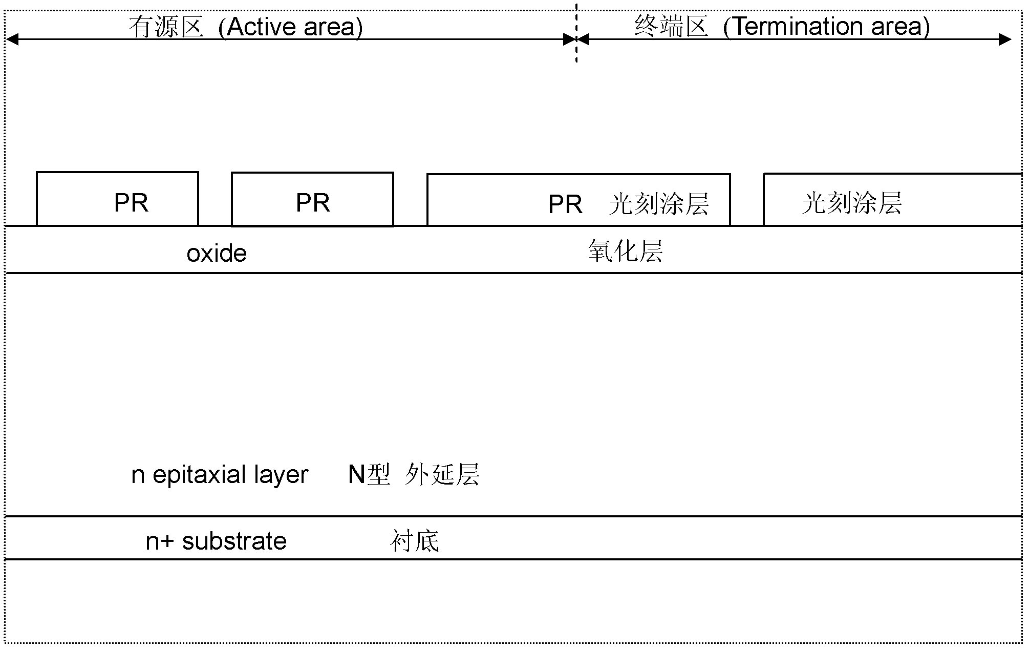
[0059] Such as figure 1 As shown, the epitaxial layer is placed above the substrate. First, an oxide layer (with a thickness of 0.3um to 1.5um oxide hard mask) is formed on the epitaxial layer by deposition or thermal growth, and another layer is deposited on the oxide layer. The photolithographic coating is then patterned through a trench mask to expose some portions of the oxide layer.

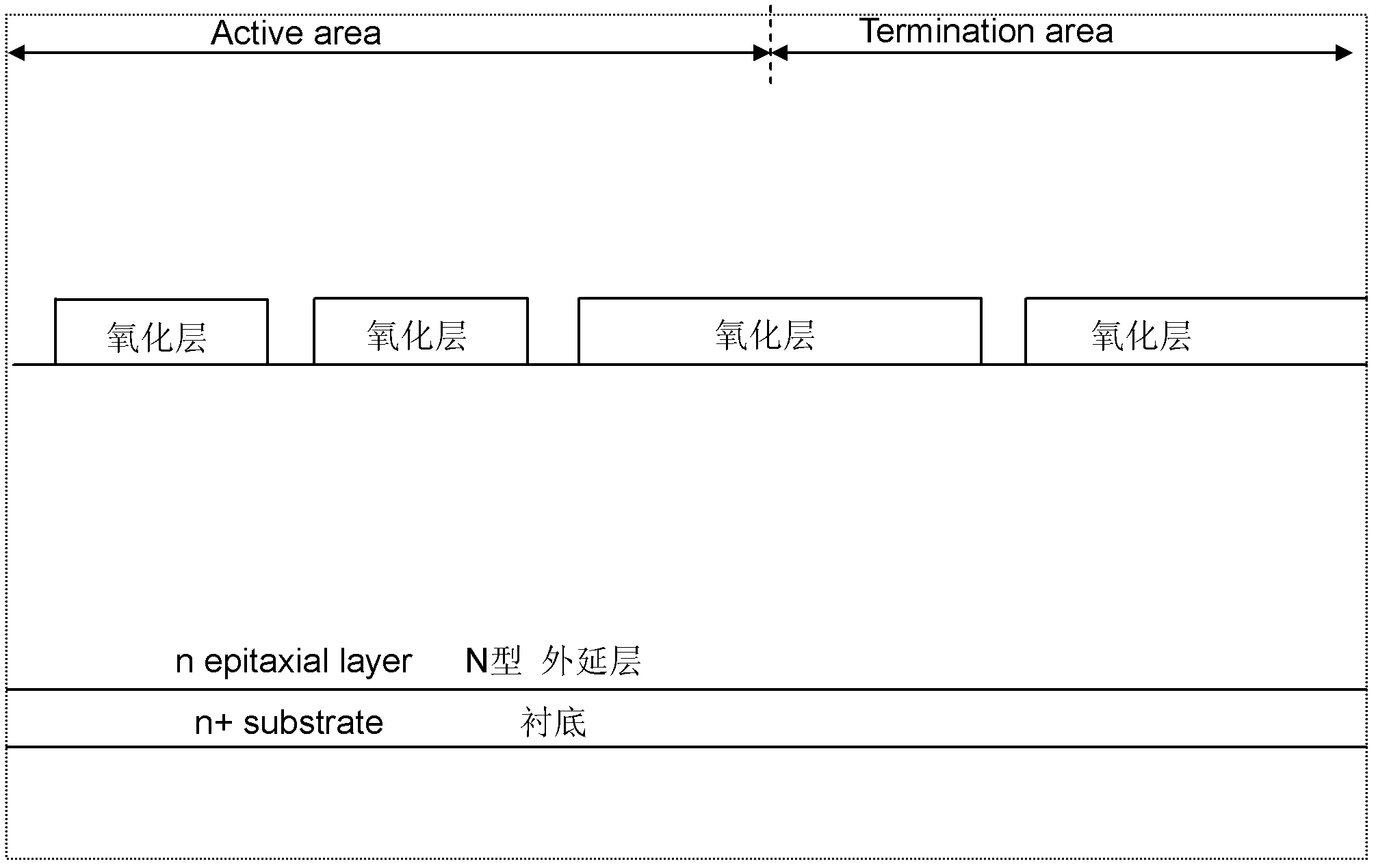
[0060] Such as figure 2 As shown, after dry etching the oxide layer exposed by patterning the trench mask, the epitaxial layer is exposed, and then the photolithographic coating is removed.

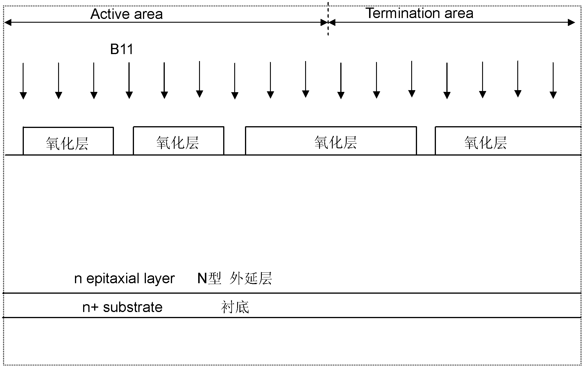
[0061] Such as image 3 As shown, implant P-type dopants on the surface of the silicon wafer (the dose is 8e12 / cm 3 to 2e14 / cm 3 ), the part covered by the original oxide layer is not implanted, and the part not covered by the original oxide layer, the P-type dopant will be implanted on the surface of the epitaxial layer to form a P-type region, and the P-type dopant can be B11 (boron boron) .

...

Embodiment 2

[0075] The technical scheme of the present embodiment is roughly the same as that of embodiment 1, and its difference only lies in:

[0076] In the above example 1 Figure 5 Before etching the trench, first deposit a layer of oxide layer and seal the opening width of the trench mask in the oxide layer ranging from 0.2um to 0.6um. The width of the sealed opening can be 0.2um or 0.3um or 0.4um or 0.5um or 0.6um varies, depending on the preparation method. The advantage of this step is that some trench mask openings are implanted with P-type dopants but not trenched. The terminal structure of the device is better, so the breakdown voltage of the device is higher and more stable. Then dry etch the oxide layer to remove the oxide layer on the opening and expose the epitaxial layer on the opening; then etch the trench, At this time, only those openings that are not sealed by the precipitated oxide layer are trenched, and the trench (1.0um to 7.0um in depth and 0.2um to 2.0um in wid...

Embodiment 3

[0078] The technical scheme of the present embodiment is roughly the same as that of embodiment 1, and its difference only lies in:

[0079] In the above example 1 Figure 13 Before etching the contact hole trench, first deposit a layer of (LPCVD) oxide layer, and then dry-etch the oxide layer to remove the oxide layer in the opening of the contact hole trench, exposing the epitaxial layer in the opening; etched contact hole trenches. Other steps are basically identical with embodiment 1 or embodiment 2, and the cross section of device is as follows Figure 17 shown.


PUM


Abstract

The invention discloses a preparation method of a trench semiconductor power discrete device. The preparation method of the trench semiconductor power discrete device includes a first step of injecting P-type dopant into an epitaxial layer arranged on a substrate to form P-type base regions through a trench mask and conducting corrosion on the epitaxial layer to form a plurality of grid trenches; a second step of depositing interlayer mediums on the epitaxial layer, conducting the corrosion on the interlayer mediums through a contact hole mask, forming trenches in the interlayer mediums, injecting N-type dopant to form N-type source regions, conducting the corrosion on the surface of the epitaxial layer to form contact trenches, and conducting metal plugging filling on the contact trenches; and a third step of depositing a metal layer on the surface of the discrete device, conducting metal corrosion through a metal mask and forming a metal substrate layer and a connecting wire. The preparation method of the trench semiconductor power discrete device eliminates preparation procedures of a base region mask and a source region mask, and therefore the manufacturing cost of the discrete device is greatly reduced. In addition, original electrical characteristics of the discrete device cannot be influenced.

Description

technical field [0001] The invention relates to the technical field of semiconductor power discrete devices, in particular to a method for preparing a trench semiconductor power discrete device. Background technique [0002] At present, the power MOSFET (Metal Oxide Semiconductor Field Effect Transistor, Metal Oxide Semiconductor Field Effect Transistor) has been widely used in various electronic and communication products, and at the same time, it also has various applications in industry. [0003] Power semiconductor devices represented by power MOSFETs can effectively control high-frequency large currents due to their low on-resistance and high-speed switching. At the same time, power MOSFETs are being widely used as small power conversion components such as power amplifiers, power converters, low noise amplifiers, and some personal computer power supply switches and power circuits, which are characterized by low power consumption and high speed. [0004] Trench power MO...

Claims


Application Information

Patent Timeline
Patent Type & Authority Applications(China)
IPC IPC(8): H01L21/336
Inventor 苏冠创
Owner 立新半导体有限公司
Why Eureka
Try Eureka