Silicon microstructure processing method based on femtosecond laser treatment and wet etching

A technology of femtosecond laser and wet etching, which is applied in the processing of silicon microstructure, deep silicon groove processing based on femtosecond laser processing and wet etching, can solve the problems of complicated process and achieve simple process and deep Large, good corrosion selectivity

Active Publication Date: 2013-08-07
XI AN JIAOTONG UNIV
View PDF6 Cites 12 Cited by
  • Summary
  • Abstract
  • Description
  • Claims
  • Application Information

AI Technical Summary

Problems solved by technology

However, this method is more complex

Method used


Image

  • Silicon microstructure processing method based on femtosecond laser treatment and wet etching
  • Silicon microstructure processing method based on femtosecond laser treatment and wet etching
  • Silicon microstructure processing method based on femtosecond laser treatment and wet etching

Examples


Embodiment 1

[0035] In this embodiment, the processing of deep silicon grooves is taken as an example, and the details are as follows:

[0036] Raw material: N-type monocrystalline silicon wafer polished on one side, crystal orientation, thickness 500μm.

[0037] The detailed implementation of the preparation steps of high aspect ratio deep silicon grooves is described as follows:

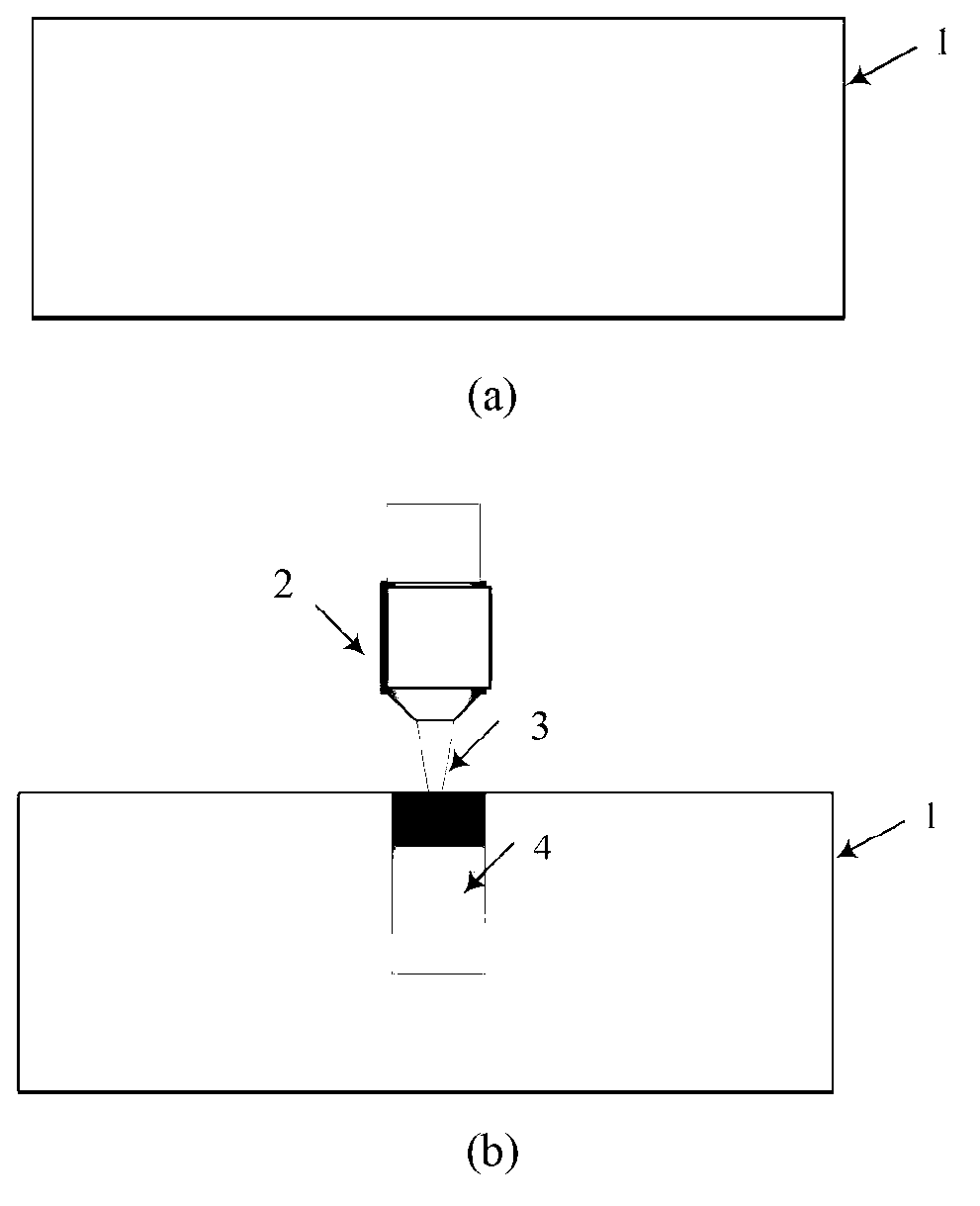
[0038] (1) Use acetone, alcohol and deionized water to carry out ultrasonic-assisted cleaning on the single crystal silicon substrate 1 in sequence, and dry it after cleaning, see figure 2 (a).

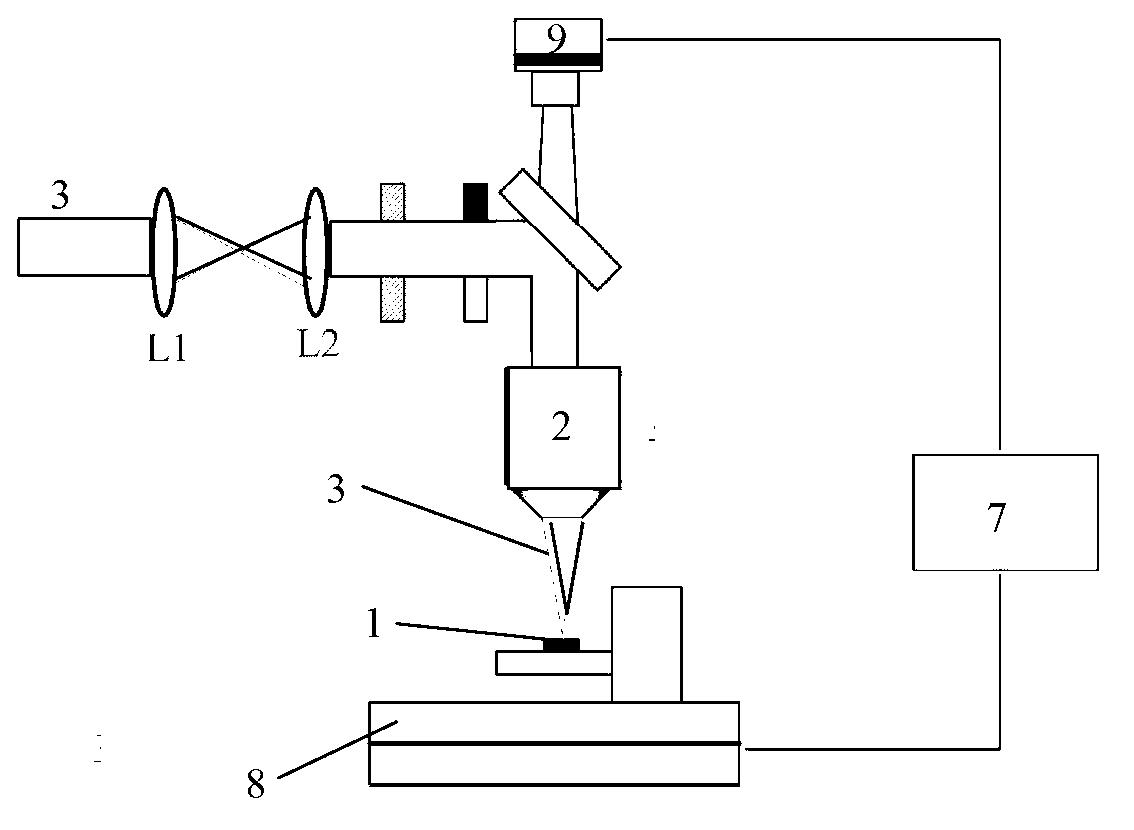
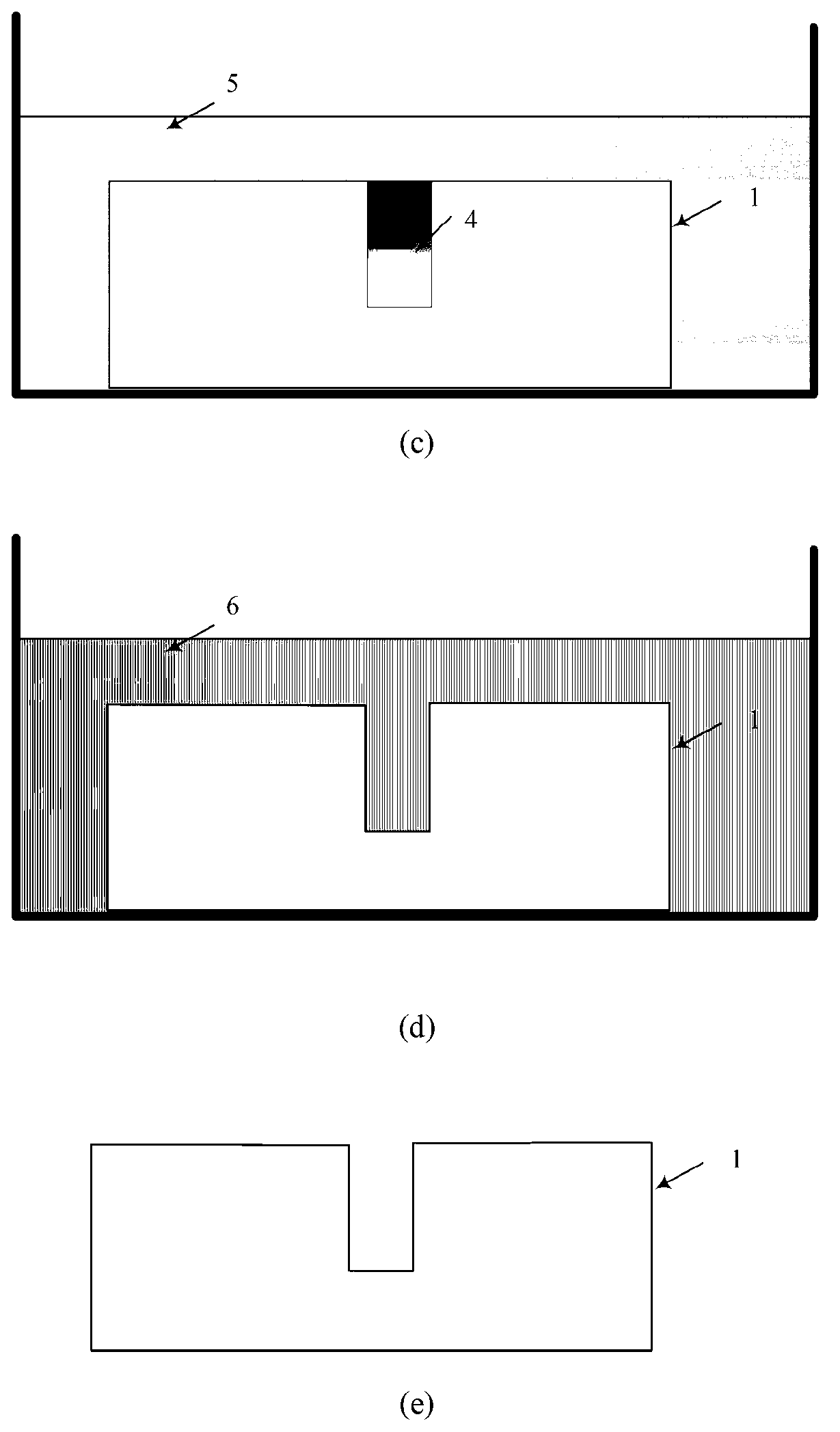
[0039] (2) The pulse width of the femtosecond laser 3 is 50 fs, and the power is set to 30 mW. A microscopic objective lens 2 with a value of 10× and a numerical aperture of 0.3 is selected to focus the femtosecond laser 3 on the single crystal silicon substrate 1 through the microscopic objective lens 2, and the scanning speed of the three-dimensional electric translation stage 8 is 2 μm / s. Use the femtosecond la...

Embodiment 2

[0043] Raw material: N-type monocrystalline silicon wafer polished on one side, crystal orientation, thickness 500μm.

[0044] (1) Cleaning of the single crystal silicon substrate 1 refers to the corresponding process of the first embodiment.

[0045] (2) The process of scanning the monocrystalline silicon substrate 1 with the femtosecond laser 3 refers to the corresponding process of Example 1, and the parameters are: the pulse width of the femtosecond laser 3 is 50 fs, and the power is set to 30 mW; A microscope objective lens 2; a three-dimensional electric translation stage 8 with a scanning rate of 2 μm / s.

[0046] (3) Corrosion of silicon wafer after scanning by femtosecond laser 3 Refer to the corresponding process of Example 1.

[0047](4) Cleaning of the silicon wafer after etching refers to the corresponding process of Example 1.

[0048] Figure 4 It is the morphology of the silicon groove finally processed in Example 2. It can be seen from the figure that the ...

Embodiment 3

[0050] Raw material: N-type monocrystalline silicon wafer polished on one side, crystal orientation, thickness 500μm.

[0051] (1) Cleaning of the single crystal silicon substrate 1 refers to the corresponding process of the first embodiment.

[0052] (2) The process of scanning the monocrystalline silicon substrate 1 with the femtosecond laser 3 refers to the corresponding process of Example 1, and the parameters are: the pulse width of the femtosecond laser 3 is 50 fs, and the power is set to 40 mW; select 10 ×, numerical aperture 0.3 A microscope objective lens 2; a three-dimensional electric translation stage 8 with a scanning rate of 2 μm / s.

[0053] (3) Corrosion of silicon wafer after scanning by femtosecond laser 3 Refer to the corresponding process of Example 1.

[0054] (4) Cleaning of the silicon wafer after etching refers to the corresponding process of Example 1.

[0055] Figure 5 It is the morphology of the silicon groove finally processed in Example 3. As ...


PUM

PropertyMeasurementUnit
thicknessaaaaaaaaaa
depthaaaaaaaaaa

Abstract

The invention discloses a silicon microstructure processing method based on femtosecond laser treatment and wet etching. The method comprises the steps of scanning a monocrystal silicon substrate by using a femtosecond laser at an oxygen-containing gas atmosphere; inducing silicon to generate refractive index change in a scanning region; and then, etching by using a hydrofluoric acid wet process to remove a refractive index change region to form a silicon microstructure. The method disclosed by the invention is simple in process; compared with the prior art, the method has the advantage that a distribution drawing of the microstructure does not need to be defined by using a mask plate; compared with the ordinary wet etching and dry etching, the method has the advantages that the corrosion selectivity is good, the etching region is completely determined by a femtosecond laser processing region, and no sidewise underetching exists; and a silicon slot with high depth-to-width ratio and large depth can be obtained during deep silicon slot processing. The method disclosed by the invention can be applied to a micro-electro-mechanical system.

Description

technical field [0001] The invention belongs to the technical fields of MEMS and semiconductor integrated circuits, and relates to a silicon microstructure processing method, in particular to a deep silicon groove processing method based on femtosecond laser processing and wet etching. Background technique [0002] In the processing of semiconductor devices and micro-mechanical electronic systems, wet etching and dry etching are mainly used to process micro-nano structures on silicon. Wet etching and dry etching generally require the use of a mask to define the etched area. Wet etching uses a solution that can chemically react with silicon to etch silicon, usually using alkali (KOH, NaOH, etc.) or acid (HF and HNO 3 mixed solution, etc.) solution. Dry etching is to use plasma to etch silicon through chemical or physical action. Anisotropic dry etching is currently the most important method for processing deep silicon trenches with high aspect ratios. [0003] Deep silico...

Claims


Application Information

Patent Timeline
Patent Type & Authority Applications(China)
IPC IPC(8): H01L21/02B81C1/00
Inventor 陈涛司金海马云灿潘安陈烽侯洵
Owner XI AN JIAOTONG UNIV
Why Eureka
Try Eureka