Method for manufacturing metal grid-graphene transparent electrode and method for manufacturing touch screen from metal grid-graphene transparent electrode
A technology of metal grids and manufacturing methods, which is applied in the direction of cable/conductor manufacturing, circuits, electrical components, etc., can solve problems such as difficult application, influence on photoelectric performance, and easy disconnection, etc., achieve excellent photoelectric performance and flexibility, and improve photoelectric performance. The effect of performance and low cost
- Summary
- Abstract
- Description
- Claims
- Application Information
AI Technical Summary
Problems solved by technology
Method used
Image

Examples
Embodiment 1
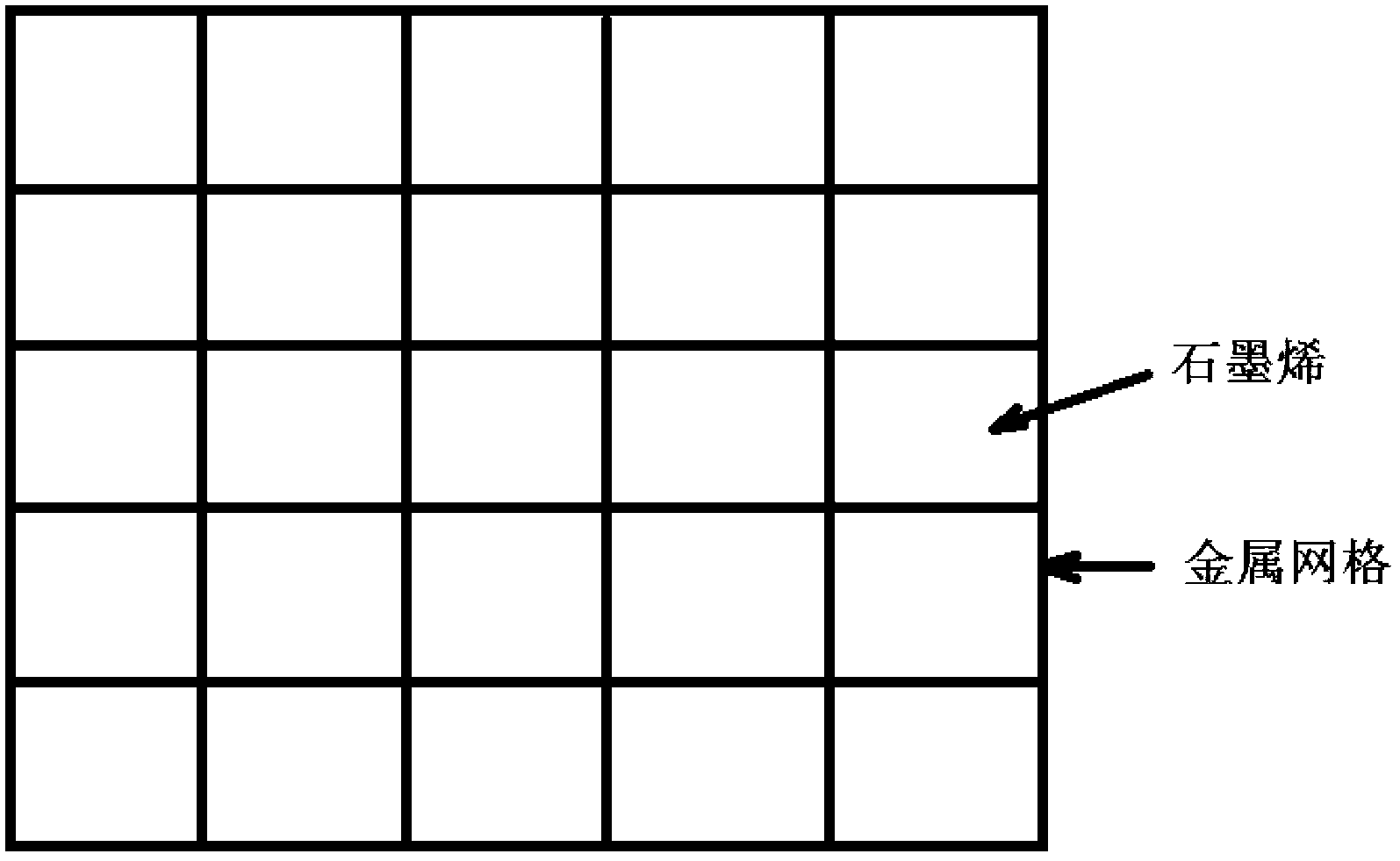
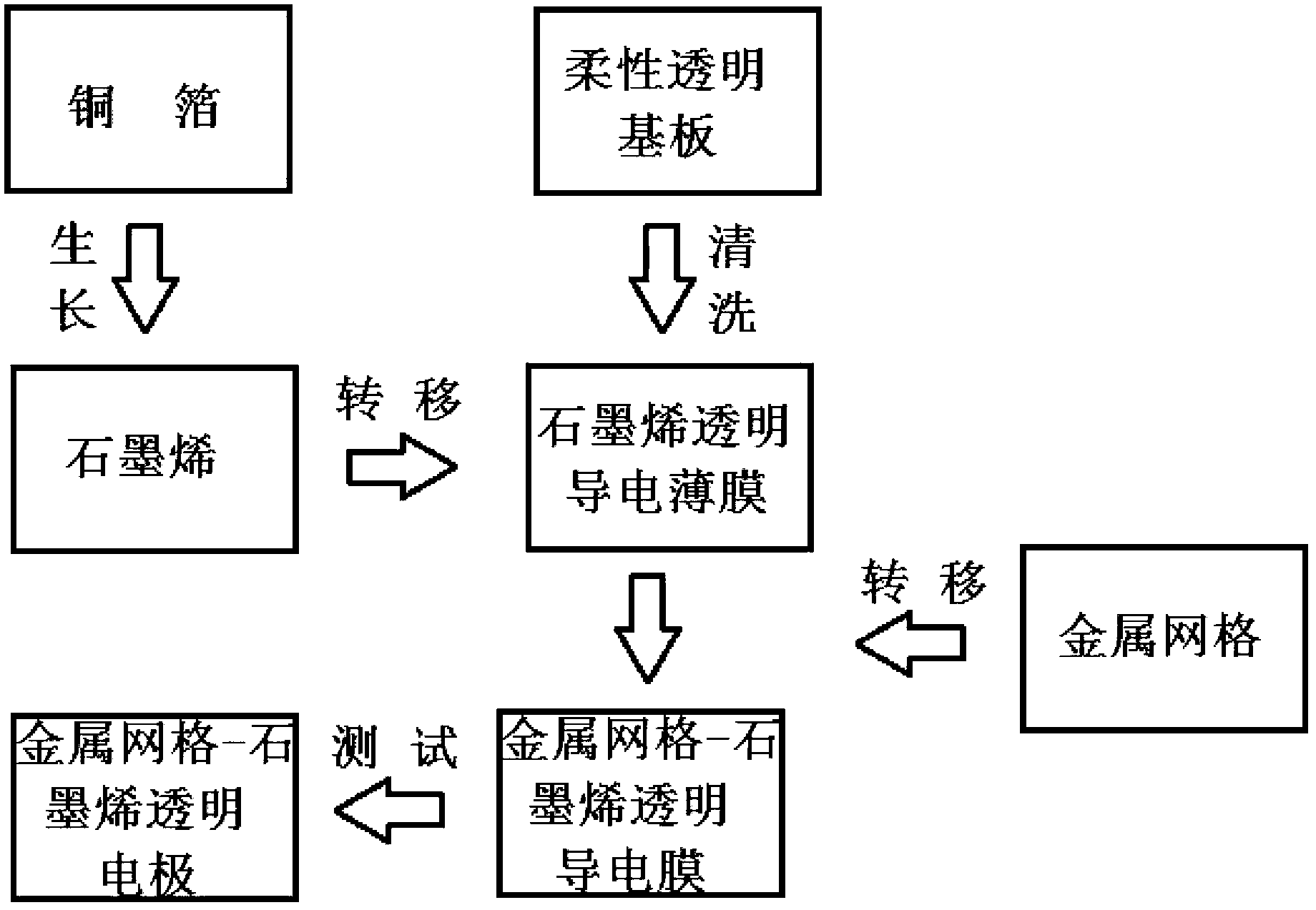
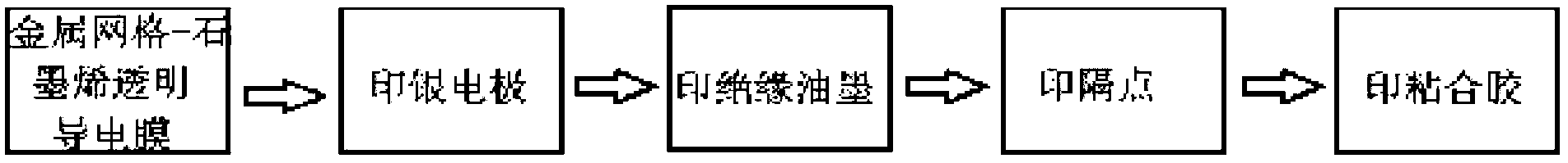
[0037] The metal material of the metal grid is Cu, the metal line width is 500um, the metal line width is 50nm, the metal thickness is 100nm, and the metal duty cycle is 19%. The periodic metal grid was prepared by photolithography, the exposure time was 1 s, and the developing time was 10 s. The material of the transparent insulating flexible substrate is PET, the square resistance is 5Ω / sq, the light transmittance is 80%, and the square resistance has no effect when the bending radius is 4mm.
[0038] Large-area graphene growth by CVD method: Graphene growth is carried out in a large-diameter tube furnace under the conditions of copper foil as a substrate and the presence of a catalyst, a gas carbon source, and a protective gas. The growth temperature is 100°C, and the growth is 1 min. The graphene grown on the copper foil is transferred to the metal grid to form a flexible metal grid-graphene transparent electrode.
Embodiment 2
[0040] The metal material of the metal grid is Ag, the metal line width is 1000um, the metal line width is 40nm, the metal thickness is 10nm, and the metal duty cycle is 10%. The periodic metal grid was prepared by photolithography, the exposure time was 600s, and the developing time was 600s. The material of the transparent insulating flexible substrate is PET, the sheet resistance is 1000Ω / sq, the light transmittance reaches 97%, and the sheet resistance has no effect when the bending radius is 1mm.
[0041] Large-area graphene growth by CVD method: Graphene growth is carried out in a large-diameter tube furnace under the conditions of copper foil as a substrate and the presence of a catalyst, a gas carbon source, and a protective gas. The growth temperature is 1100°C, and the growth is 60 minutes. The graphene grown on the copper foil is transferred to the metal grid to form a flexible metal grid-graphene transparent electrode.
Embodiment 3
[0043]The metal material of the metal grid is Au, the metal line width is 500um, the metal line width is 4um, the metal thickness is 100nm, and the metal duty cycle is 10%. The periodic metal grid was prepared by photolithography, the exposure time was 3 min, and the developing time was 60 s. The material of the transparent insulating flexible substrate is PET, the sheet resistance is 100Ω / sq, the light transmittance is 90%, and the sheet resistance has no effect when the bending radius is 4mm.
[0044] Large-area graphene growth by CVD method: Graphene growth is carried out in a large-diameter tube furnace under the conditions of copper foil as a substrate and the presence of a catalyst, a gas carbon source, and a protective gas. The growth temperature is 500°C, and the growth is 20 minutes. The graphene grown on the copper foil is transferred to the metal grid to form a flexible metal grid-graphene transparent electrode.
[0045] Some experimental results of the photoelectr...
PUM
| Property | Measurement | Unit |
|---|---|---|
| Line width | aaaaa | aaaaa |
| Thickness | aaaaa | aaaaa |
| Resistance | aaaaa | aaaaa |
Abstract
Description
Claims
Application Information
 - R&D
- Intellectual Property
- Life Sciences
- Materials
- Tech Scout
- Unparalleled Data Quality
- Higher Quality Content
- 60% Fewer Hallucinations
Browse by: Latest US Patents, China's latest patents, Technical Efficacy Thesaurus, Application Domain, Technology Topic, Popular Technical Reports.
© 2025 PatSnap. All rights reserved.Legal|Privacy policy|Modern Slavery Act Transparency Statement|Sitemap|About US| Contact US: help@patsnap.com