Polycrystalline silicon thin film transistor based on solid-phase crystallization technology and manufacturing method thereof
A polysilicon thin film and a manufacturing method technology, applied in transistors, semiconductor/solid-state device manufacturing, semiconductor devices, etc., can solve problems such as many defects, high TFT threshold voltage, and small sub-threshold slope.
- Summary
- Abstract
- Description
- Claims
- Application Information
AI Technical Summary
Problems solved by technology
Method used
Image
Examples
Embodiment 1
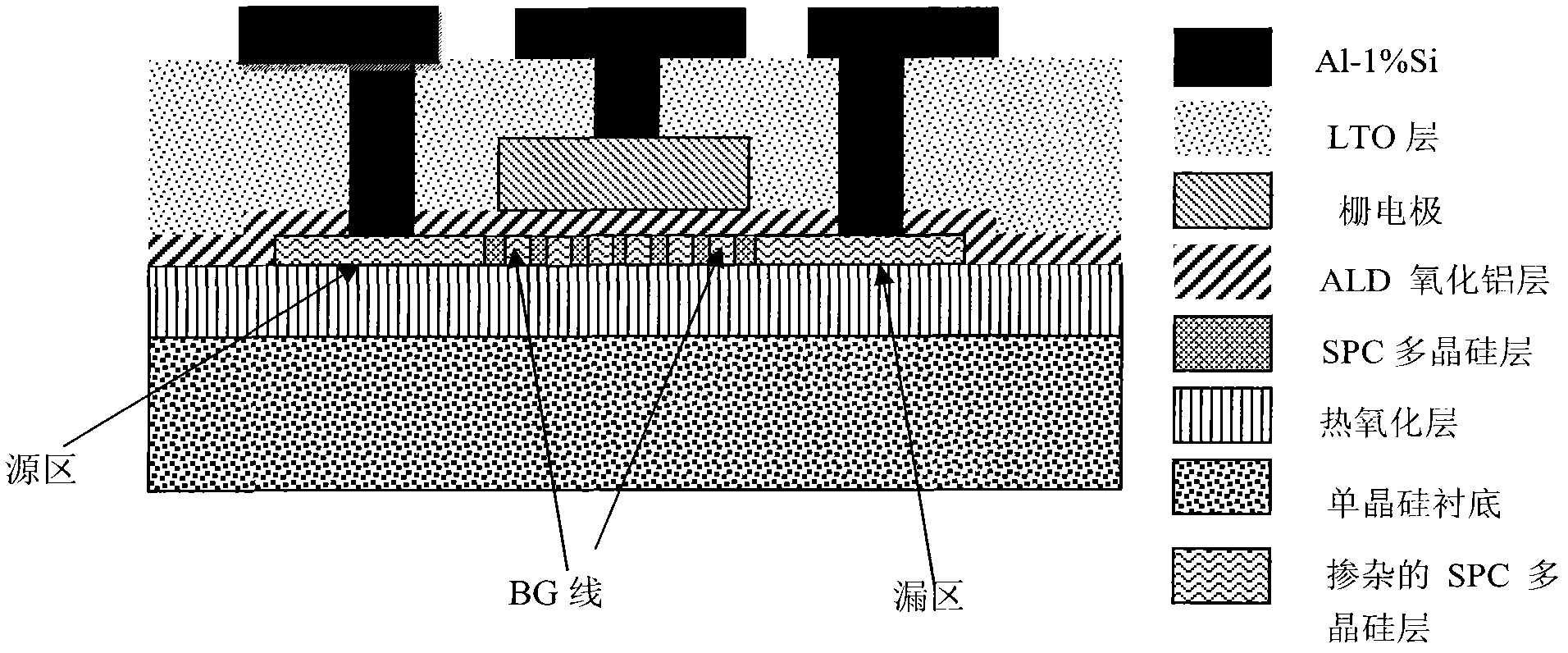
[0022] This embodiment provides a figure 1 TFTs shown, including:
[0023] Monocrystalline silicon wafer substrate;
[0024] Thermal silicon oxide layer on the substrate; 100nm thick polysilicon layer on the thermal silicon oxide layer, formed by SPC (solid phase crystallization) process, as the active layer of the transistor, with boron-doped bridging grains in the active layer (BG) lines, the width of BG lines is 0.5 μm, the distance between BG lines is 0.5 μm, and the doping density of boron ions is 2×10 15 / cm 2 , the polysilicon layer also has a source region and a drain region, a plurality of BG lines are parallel, and the parallel BG lines are perpendicular to the current direction.
[0025] Aluminum oxide (Al 2 o 3 ) layer, with a thickness of 47nm, used as a gate dielectric layer;
[0026] A gate electrode on the gate dielectric layer, wherein the channel width-to-length ratio (W / L) is 24 μm / 10 μm;
[0027] LTO (low temperature oxide, low temperature deposited ...
Embodiment 2
[0030] This embodiment provides a method for manufacturing the polysilicon thin film transistor provided in Embodiment 1, including: 1) covering the surface of a single crystal silicon substrate with 500nm thermal silicon oxide; 2) by low pressure chemical vapor deposition (LPCVD) Deposit 100nm amorphous silicon active layer; 3) perform SPC (solid phase crystallization) process: single crystal silicon substrate in N 2 Anneal at 600C for 24 hours to crystallize the amorphous silicon to form a polysilicon active layer; 4) Spin coat a layer of PR1075 photoresist on the surface of the polysilicon active layer, and then heat to 90 degrees for soft baking. The heating time is For 1 minute, the photoresist was exposed to light with a wavelength of 365nm, baked at 110°C for 1 minute, and then the sample was soaked in FHD-5 (2.38%TMAH) for 30 seconds for development, and the photoresist exposed to light The glue is dissolved in the developer solution, and the part that is not exposed t...
PUM
| Property | Measurement | Unit |
|---|---|---|
| Thickness | aaaaa | aaaaa |
| Thickness | aaaaa | aaaaa |
| Roughness | aaaaa | aaaaa |
Abstract
Description
Claims
Application Information


