High efficient three-lamination-layer heterojunction film solar cell and preparation method thereof

A solar cell and heterojunction technology, applied in the field of solar cells, can solve the problems of low efficiency and achieve the effects of simple preparation equipment, stable electrical performance, and easy-to-master process

Active Publication Date: 2013-09-25
北京大昱光伏科技有限公司
View PDF4 Cites 12 Cited by
  • Summary
  • Abstract
  • Description
  • Claims
  • Application Information

AI Technical Summary

Problems solved by technology

The development of silicon-based thin-film solar cells is from single-junction a-Si to double-junction microcrystalline silicon germanium μc-Si / μc-SiGe, the optical band gap of μc-Si / μc-SiGe cells is 1.1-1.25eV, and its conversion rate is only It is 10%, and the efficiency is low, which needs to be further improved after technological innovation, so as to reduce the unit cost; while CuInSe 2 It is a compound semiconductor material with a direct bandgap, which has an ideal optical bandgap value of up to 1.04eV. If CuInSe 2 Combined application to Si-based thin-film solar cells to make a heterojunction thin-film solar cell with a three-layer structure can not only expand the absorption wavelength range of sunlight, improve photoelectric conversion efficiency, but also reduce unit cost, but how to combine the two Application has always been a difficult problem in the industry, and it still needs to be explored and innovated

Method used


Image

  • High efficient three-lamination-layer heterojunction film solar cell and preparation method thereof

Examples


Embodiment Construction

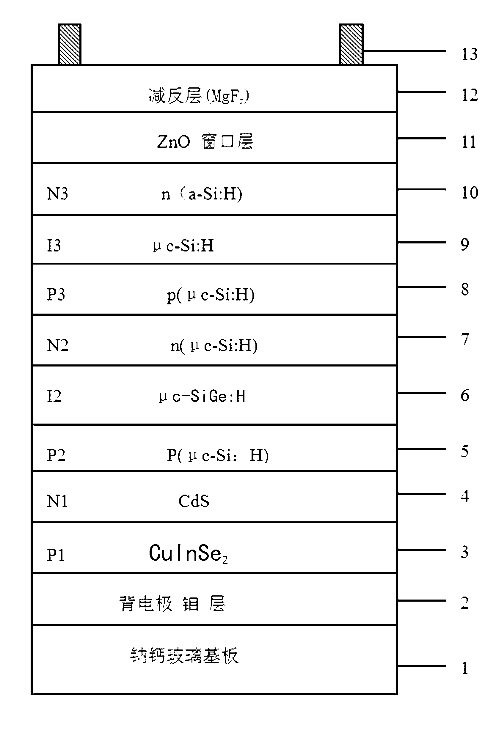
[0013] The high-efficiency triple-layer heterojunction thin-film solar cell of the present invention is provided with three-junction stacked sub-cells connected in series, the first junction is the bottom cell, which is a PN junction structure composed of P1 layer 3 and N1 layer 4, and the P1 layer is CuInSe 2 material, the N1 layer is CdS material; the second junction is a medium battery, which is a NIP structure composed of P2 layer 5, I2 layer 6, and N2 layer 7. The P2 layer is μ-Si: H-doped trimethyl boron material, and the I2 layer is The light absorption layer is made of microcrystalline silicon germanium μc-SiGe material, and the N2 layer is μ-Si:H doped phosphine material; the third junction is the top cell, which is a NIP structure composed of P3 layer 8, I3 layer 9, and N3 layer 10. The P3 layer is μ-Si: H-doped trimethyl boron material, the I3 layer is a light absorbing layer using microcrystalline silicon μc-Si material, and the N3 layer is a-Si: H-doped phosphine m...


PUM


Abstract

The utility model provides a high efficient three-lamination-layer heterojunction film solar cell which comprises three sub cells in stacked series connection. The first sub cell is a bottom cell which is a PN junction structure formed by a P1 layer and an N1 layer, the P1 layer is a CuInSe2 material, and the N1 layer is a CdS material. The second cell is a middle cell, the third cell is a top cell, and both the second cell and the third cell are NIP structures. A transition layer with the 10nm thickness is arranged between the first cell and the second cell. A intrinsic amorphous silicon material is employed, contact interfaces of the transition layer with the first cell and the second cell are subjected to processing of plasma bombardment. A SiOx intermediate layer is plated between the second cell and the third cell. The first cell is plated on a glass substrate with a back electrode molybdenum layer. The top of the third cell is orderly plated with a conductive window layer, an antireflection layer and a gate electrode. According to the high efficient three-lamination-layer heterojunction film solar cell, the photoelectric conversion efficiency is raised, the unit cost is effectively reduced, the structure performance of the cell is stable, and the stability of electrical properties in long-term use can be ensured.

Description

technical field [0001] The invention relates to a solar cell, in particular to a high-efficiency triple-layer heterojunction thin-film solar cell and a preparation method thereof. Background technique [0002] Si-based thin-film solar cells have the advantages of high sunlight absorption coefficient, small temperature coefficient affecting cell efficiency, low production cost, and suitable for large-scale large-scale production. It is the film with the highest degree of industrialization and the largest actual production scale among all thin-film solar cells. Solar battery. The development of silicon-based thin-film solar cells is from single-junction a-Si to double-junction microcrystalline silicon germanium μc-Si / μc-SiGe, the optical band gap of μc-Si / μc-SiGe cells is 1.1-1.25eV, and its conversion rate is only It is 10%, and the efficiency is low, which needs to be further improved after technological innovation, so as to reduce the unit cost; while CuInSe 2 It is a com...

Claims


Application Information

Patent Timeline
Patent Type & Authority Applications(China)
IPC IPC(8): H01L31/078H01L31/0272H01L31/20
CPCY02E10/50Y02P70/50
Inventor 董德庆李朗川信德磊付东东
Owner 北京大昱光伏科技有限公司
Why Eureka
Try Eureka