High-efficiency triple-layer heterojunction thin-film solar cell and its preparation method
A solar cell and heterojunction technology, applied in the field of solar cells, can solve problems such as low efficiency, and achieve the effects of simple preparation equipment, low manufacturing cost, and lower unit cost
- Summary
- Abstract
- Description
- Claims
- Application Information
AI Technical Summary
Problems solved by technology
Method used
Image
Examples
Embodiment Construction
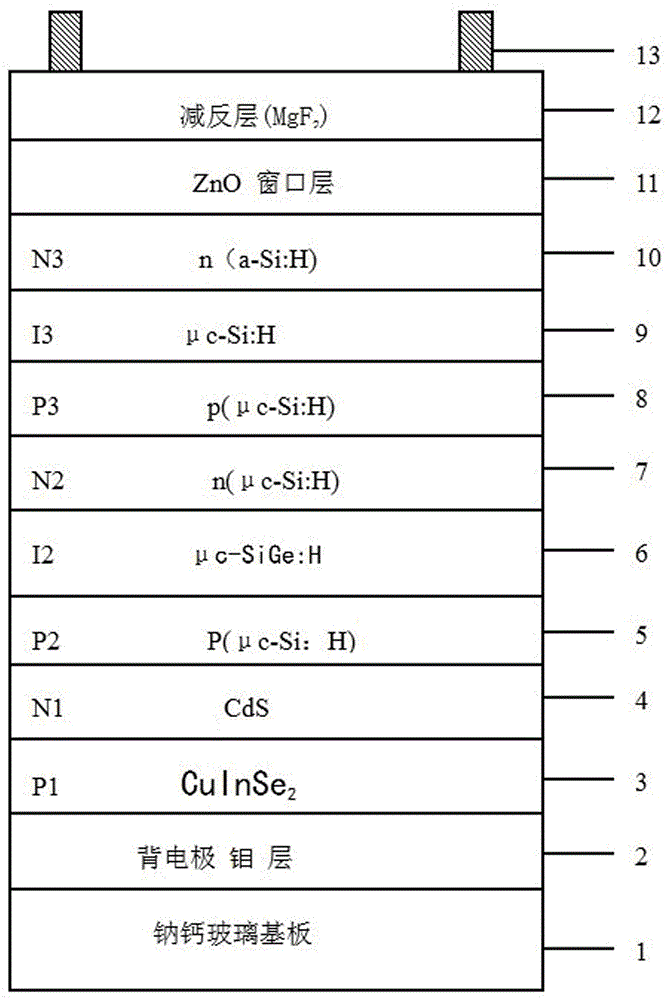
[0013] The high-efficiency triple-layer heterojunction thin-film solar cell of the present invention is provided with three-junction stacked sub-cells connected in series, the first junction is the bottom cell, which is a PN junction structure composed of P1 layer 3 and N1 layer 4, and the P1 layer is CuInSe 2 material, N1 layer is CdS material; the second junction is a medium battery, which is a NIP structure composed of P2 layer 5, I2 layer 6, and N2 layer 7, and the P2 layer is μc-Si:H-doped trimethyl boron material, and the I2 layer is The light absorbing layer is made of microcrystalline silicon germanium μc-SiGe material, and the N2 layer is μc-Si:H doped phosphine material; the third junction is the top cell, which is a NIP structure composed of P3 layer 8, I3 layer 9, and N3 layer 10. The P3 layer is μc-Si: H-doped trimethyl boron material, the I3 layer is a light absorbing layer using microcrystalline silicon μc-Si material, and the N3 layer is a-Si: H-doped phosphine ...
PUM
 Abstract
Description
Claims
Application Information
