

A kind of fabrication method of electric injection gan-based resonator
A manufacturing method and resonant cavity technology, applied in the field of GaN-based resonant cavity light-emitting devices, can solve the problems of difficult lateral expansion of holes, decrease of cavity quality factor, and affecting the performance of resonant cavity, so as to achieve good electrical and optical characteristics and improve Q value, performance-enhancing effects
- Summary
- Abstract
- Description
- Claims
- Application Information
AI Technical Summary
Problems solved by technology
Method used
Image

Examples
Embodiment Construction
[0022] In order to make the purpose, technical solution and advantages of the present invention clearer, the present invention will be further described in detail by taking GaN-based RCLED as an example and referring to the accompanying drawings.
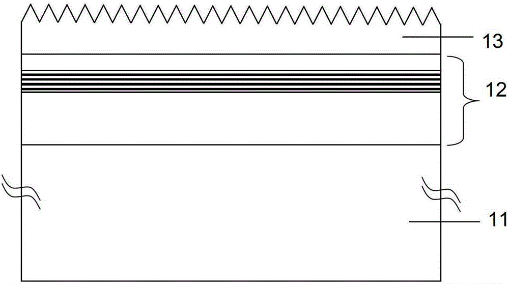
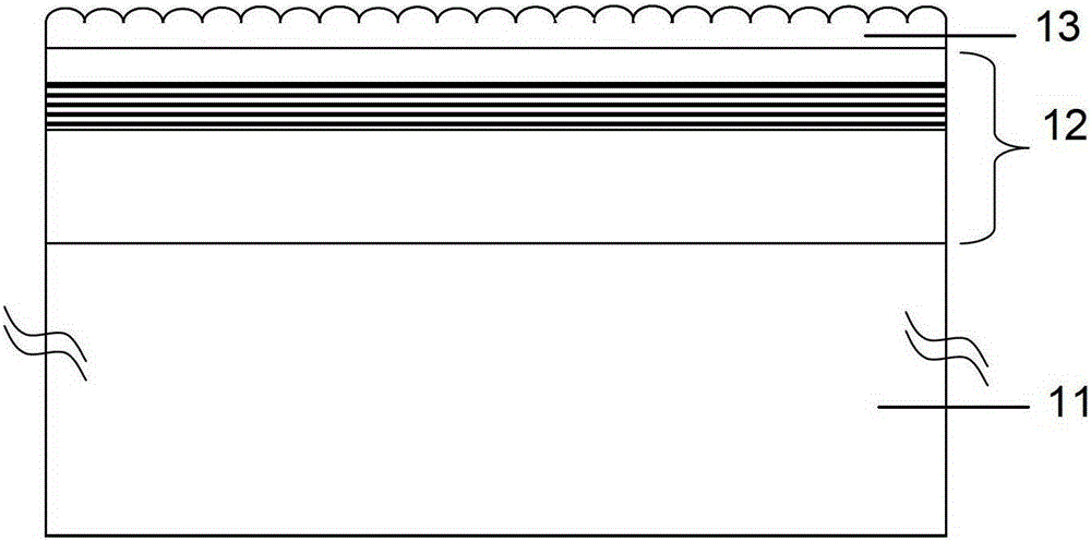
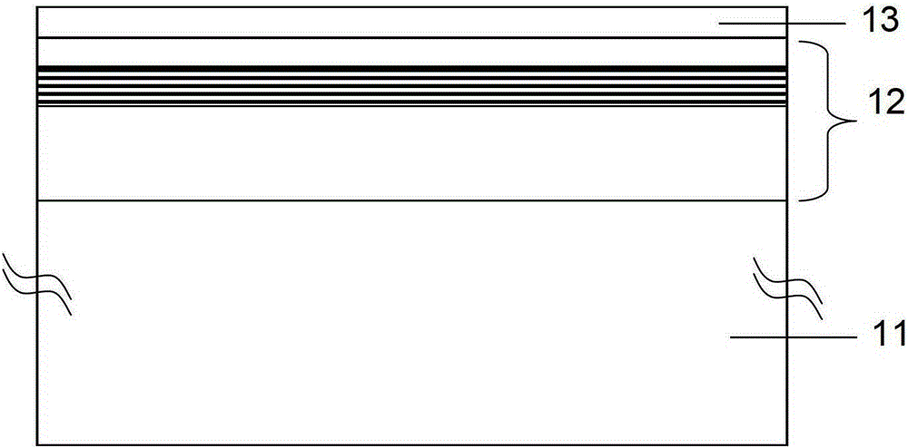
[0023] see Figure 1-9 , the embodiment of the present invention includes the following steps:
[0024] 1) Using the MOCVD method on the sapphire substrate 11, a low-temperature buffer layer, an undoped GaN buffer layer, a Si-doped GaN layer, an InGaN / GaN multi-quantum well active layer, a Mg-doped AlGaN layer and a Mg-doped GaN-based epitaxial layer 12 such as a GaN layer, and high-temperature annealing is performed after the growth of the epitaxial wafer is completed to increase the hole concentration;
[0025] 2) A p-type current spreading layer ITO13 with a thickness of 250nm was prepared on the above-mentioned epitaxial wafer by electron beam evaporation equipment. The AFM scanning image of the grown ITO surface is as follows ...
PUM
| Property | Measurement | Unit |
|---|---|---|
| Thickness | aaaaa | aaaaa |
| Thickness | aaaaa | aaaaa |
| Surface roughness | aaaaa | aaaaa |
Abstract
Description
Claims
Application Information