Method for transplanting silicon nanowire array and preparing simple device thereof

A technology of silicon nanowire arrays and nanowire arrays, which is applied in the field of silicon nanowire array device manufacturing, can solve problems such as limiting the scope of application, and achieve the effects of simple operation, good ohmic contact, and low cost

Inactive Publication Date: 2013-10-02
HEFEI INSTITUTES OF PHYSICAL SCIENCE - CHINESE ACAD OF SCI
View PDF4 Cites 11 Cited by
  • Summary
  • Abstract
  • Description
  • Claims
  • Application Information

AI Technical Summary

Problems solved by technology

[0003] The method of preparing silicon nanowire arrays in the prior art is mainly through physical or chemical methods, such as reactive ion etching and wet che

Method used


Image

  • Method for transplanting silicon nanowire array and preparing simple device thereof
  • Method for transplanting silicon nanowire array and preparing simple device thereof
  • Method for transplanting silicon nanowire array and preparing simple device thereof

Examples


specific Embodiment approach

[0030] The implantation of the silicon nanowire array and the simple device preparation method of the present invention, the preferred specific embodiments thereof are:

[0031] Include steps:

[0032] A. Silicon wafer pretreatment: cleaning single crystal silicon wafer;

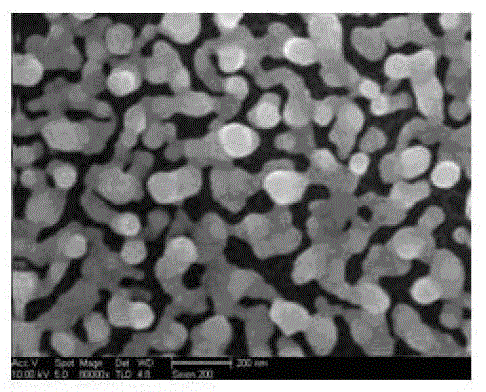
[0033] B. Preparation of porous silver film on silicon wafer: put the cleaned silicon wafer in step A into a mixed solution of silver nitrate and hydrofluoric acid, and deposit a silver film by standing to obtain a silicon wafer with a porous silver film on the surface;

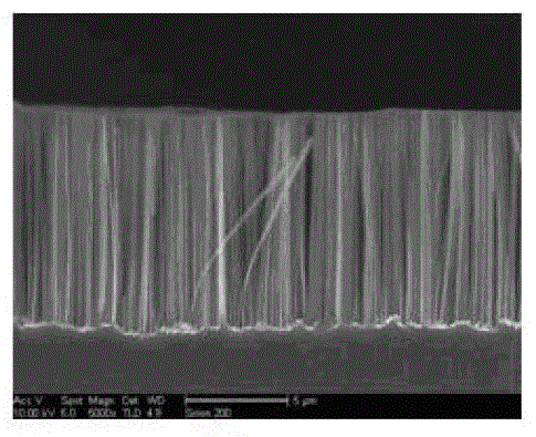
[0034] C. Preparation of silicon nanowire arrays on silicon wafers: put the silicon wafers with porous silver film on the surface obtained in step B into a mixed etching solution of hydrofluoric acid and hydrogen peroxide for static etching to obtain silicon nanowire arrays on the surface Structural silicon wafers;

[0035] D. Preparation of silicon-silicon oxide core-shell nanowire array structure: put the silicon wafer with silicon nano...

specific Embodiment

[0061] Equipment used: ultrasonic instrument, constant temperature water tank, spin coating apparatus and plasma cleaning machine.


PUM


Abstract

The invention discloses a method for transplanting a silicon nanowire array and preparing a simple device thereof. A multihole silver film prepared on a clean silicon wafer is utilized to act as catalytic metal; the silicon nanowire array is prepared through etching the multihole silver film in hydrofluoric acid or hydrogen peroxide; a silicon-silicon oxide core-shell structure is formed by oxidizing the silicon nanowire array in high-temperature water vapors; the silicon-silicon oxide core-shell structure is placed in a high-temperature aqueous solution of ammonia, and a silicon nanowire array structure detached from a silicon lining is prepared through silicon oxide blocking and silver assisted ammonia water etching. Transplantation of the nanowire array is realized by utilizing a target substrate whose surface is coated by an adhesive material; or an insulating material is used to fix and support the silicon nanowire array and acts as an intermediate insulating layer, the silicon nanowire array is transplanted to a flexible substrate whose surface is coated by a conducting adhesive material, and another layer of a conductive material is covered so as to prepare a simple and flexible breakover circuit device with good ohmic contact. The method disclosed by the invention is simple to operate and low in cost, and can be applied to mass production.

Description

technical field [0001] The invention relates to a fabrication technology of silicon nanowire array devices, in particular to a method for transplanting a silicon nanowire array and a simple device fabrication method. Background technique [0002] Due to its very large surface-to-body ratio and unique electronic and optical properties, silicon nanowire arrays have important application prospects in photovoltaics, light detection, sensors, optics and flexible electronic devices. [0003] The methods of preparing silicon nanowire arrays in the prior art are mainly through physical or chemical methods, such as reactive ion etching and wet chemical etching, etc. The common point of these methods is that the nanowires are grown on rigid substrates. , thus severely limiting its application range. Therefore, the development of simple and efficient silicon nanowire array transplantation technology is crucial. SUMMARY OF THE INVENTION [0004] The purpose of the present invention ...

Claims


Application Information

Patent Timeline
IPC IPC(8): H01L21/02B82Y40/00
Inventor 吴摞滕大勇李淑鑫何微微叶长辉
Owner HEFEI INSTITUTES OF PHYSICAL SCIENCE - CHINESE ACAD OF SCI
Why Eureka
Try Eureka