Artificial magnetic conductor shaped like Chinese character 'jing' and used for 60GHz on-chip antenna and implement method

An artificial magnetic conductor and well-shaped technology, which is used in semiconductor devices, antenna supports/installation devices, semiconductor/solid-state device manufacturing, etc. small effect

Inactive Publication Date: 2013-10-09
NANKAI UNIV
View PDF4 Cites 6 Cited by
  • Summary
  • Abstract
  • Description
  • Claims
  • Application Information

AI Technical Summary

Problems solved by technology

[0007] The purpose of the present invention is to solve the problem of silicon substrate electromagnetic wave loss for the design of 60 GHz millimeter-wave integrated circuits and on-chip antennas, to provide a well-shaped ...

Method used


Image

  • Artificial magnetic conductor shaped like Chinese character 'jing' and used for 60GHz on-chip antenna and implement method
  • Artificial magnetic conductor shaped like Chinese character 'jing' and used for 60GHz on-chip antenna and implement method
  • Artificial magnetic conductor shaped like Chinese character 'jing' and used for 60GHz on-chip antenna and implement method

Examples


Embodiment 1

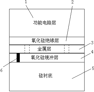
[0035] Such as figure 1 As shown, the well-shaped artificial magnetic conductor for 60 GHz on-chip antenna provided by the present invention, the specific structure includes:

[0036] Silicon substrate, silicon oxide buffer layer, metal layer, silicon oxide insulating layer and functional circuit layer are stacked and fabricated sequentially from bottom to top. The silicon substrate is located below, and it is covered with a silicon oxide buffer layer, and a metal layer is vapor-deposited on the silicon oxide buffer layer to form a distributed well-shaped structure, and a silicon oxide insulating layer is covered on the metal layer. The upper surface of the silicon insulating layer is a functional circuit layer.

[0037] The well-shaped artificial magnetic conductor is realized by traditional CMOS technology.

[0038] When the thickness of the silicon substrate is in the range of 280 microns to 320 microns, it meets the parameter requirements of the artificial magnetic cond...

Embodiment 2

[0044] The method for realizing the well-shaped artificial magnetic conductor used for 60 gigahertz on-chip antenna provided by the present invention, passes through the following steps successively:

[0045] First, prepare the silicon substrate 5 with the silicon chip of the epitaxial layer as the artificial magnetic conductor;

[0046] Second, a silicon oxide buffer layer 4 is grown on the silicon substrate 5 by a CMOS field oxidation process as the lower dielectric layer of the artificial magnetic conductor;

[0047] Third, anneal the silicon wafer, perform chemical vapor deposition oxidation on the silicon oxide buffer layer 4, and then use the first metal layer of the CMOS process to evaporate the metal layer 3;

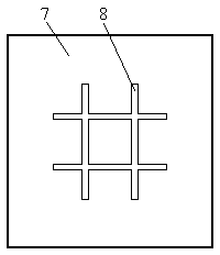
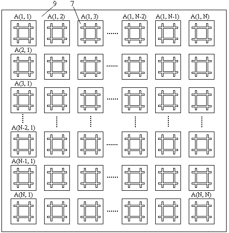
[0048] Fourth, photoetching the metal layer 3 to form a periodic array structure 9 of well-shaped small metal sheets 7, such as figure 2 and image 3 As shown, a small metal sheet 7 is fabricated on the metal layer 3, and well-shaped slots are etched on the s...

Embodiment 3

[0053] Such as image 3 As shown, the well-shaped artificial magnetic conductor for 60 GHz on-chip antenna arranged in an N×N periodic structure is specifically realized as follows:

[0054]Taking N=7, realizing a 7×7 periodic structure arrangement of a well-shaped artificial magnetic conductor for a 60 GHz on-chip antenna.

[0055] A silicon wafer with an epitaxial layer is used as the silicon substrate 5 of the well-shaped artificial magnetic conductor, and the thickness of the silicon substrate 5 is 300 microns.

[0056] The silicon oxide buffer layer 4 is grown on the silicon substrate 5 with the field oxidation process of CMOS, and the size of the silicon oxide buffer layer 4 is determined to be a square with a side length of 1.84 millimeters by means of photolithography, as the bottom of the well-shaped artificial magnetic conductor. medium layer.

[0057] Anneal the silicon wafer, perform chemical vapor deposition oxidation on the silicon oxide buffer layer 4, and the...


PUM

PropertyMeasurementUnit
Thicknessaaaaaaaaaa

Abstract

Provided is an artificial magnetic conductor shaped like a Chinese character 'jing' and used for a 60GHz on-chip antenna. The artificial magnetic conductor can be used on a millimeter wave integrated circuit, waveguide transmission, the on-chip antenna and the like. The artificial magnetic conductor is manufactured through a CMOS integrated circuit process, and is composed of a silicon substrate, a silicon oxide buffering layer, a metal layer, a silicon oxide insulation layer and an upper functional circuit layer, and the metal layer is manufactured to be of a distributed-type structure shaped like the Chinese character 'jing'. The artificial magnetic conductor is applied to the design of the millimeter wave integrated circuit and particularly the integrated on-chip antenna, effective isolation of the antenna and the silicon substrate is achieved, and incident electromagnetic waves of the antenna are prevented from entering the silicon substrate. The artificial magnetic conductor shaped like the Chinese character 'jing' and used for the 60GHz on-chip antenna serves as an isolation layer between the millimeter wave on-chip radiating antenna and the silicon substrate, the structure is simple, the CMOS process is compatible, the artificial magnetic conductor is applied to the 60GHz on-chip antenna, and loss of signals of the incident electromagnetic waves of the antenna by the silicon substrate can be reduced.

Description

technical field [0001] The present invention relates to the technical field of millimeter-wave integrated circuits and on-chip antennas, in particular to an artificial magnetic conductor structure for a 60 GHz on-chip antenna and its realization method. Background technique [0002] The short-range wireless communication in the 60 GHz frequency band has revolutionized wireless personal area networks (WPANs), in wireless consumer electronics, high-resolution and large-capacity media file transmission, mobile distributed computing, wireless games and fast transmission of large files and other fields have huge market prospects. The free space wavelength of the 60 GHz frequency is only 5 millimeters, so the wireless data transmission and reception can be realized with a very small antenna. Therefore, integrating low-noise amplifiers, mixers, frequency converters, detectors, modulators, transceivers and antennas on a single integrated circuit chip to achieve wireless communicat...

Claims


Application Information

Patent Timeline
IPC IPC(8): H01L23/552H01L23/66H01Q1/22H01L21/02
Inventor 耿卫东宋芃霖
Owner NANKAI UNIV
Why Eureka
Try Eureka