Tic-shaped artificial magnetic conductor for 60 GHz on-chip antenna and its realization method
A technology of artificial magnetic conductor and square shape, which is applied in semiconductor devices, antenna supports/mounting devices, semiconductor/solid-state device manufacturing, etc., can solve the problems of silicon substrate electromagnetic wave loss, etc., and achieve relatively large bandwidth, small area, and structure simple effect
- Summary
- Abstract
- Description
- Claims
- Application Information
AI Technical Summary
Problems solved by technology
Method used
Image
Examples
Embodiment 1
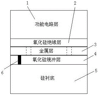
[0030] like figure 1 As shown, the well-shaped artificial magnetic conductor for 60 GHz on-chip antenna provided by the present invention, the specific structure includes:
[0031] Silicon substrate, silicon oxide buffer layer, metal layer, silicon oxide insulating layer and functional circuit layer are stacked and fabricated sequentially from bottom to top. The silicon substrate is located below, and it is covered with a silicon oxide buffer layer, and a metal layer is vapor-deposited on the silicon oxide buffer layer to form a distributed well-shaped structure, and a silicon oxide insulating layer is covered on the metal layer. The upper surface of the silicon insulating layer is a functional circuit layer.
[0032] The well-shaped artificial magnetic conductor is realized by traditional CMOS technology.
[0033] When the thickness of the silicon substrate is in the range of 280 microns to 320 microns, it meets the parameter requirements of the artificial magnetic conduct...
Embodiment 2
[0038] The method for realizing the well-shaped artificial magnetic conductor used for 60 gigahertz on-chip antenna provided by the present invention, passes through the following steps successively:
[0039] First, prepare the silicon substrate 5 with the silicon chip of the epitaxial layer as the artificial magnetic conductor;
[0040] Second, a silicon oxide buffer layer 4 is grown on the silicon substrate 5 by a CMOS field oxidation process as the lower dielectric layer of the artificial magnetic conductor;
[0041] Third, anneal the silicon wafer, perform chemical vapor deposition oxidation on the silicon oxide buffer layer 4, and then use the first metal layer of the CMOS process to evaporate the metal layer 3;
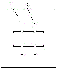
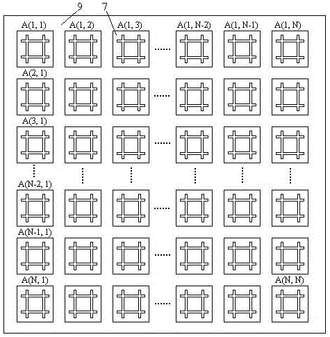
[0042] Fourth, photoetching the metal layer 3 to form a periodic array structure 9 of well-shaped small metal sheets 7, such as figure 2 and image 3 As shown, a small metal sheet 7 is fabricated on the metal layer 3, and well-shaped slots are etched on the sm...
Embodiment 3
[0046] like image 3 As shown, the well-shaped artificial magnetic conductor for 60 GHz on-chip antenna arranged in an N×N periodic structure is specifically realized as follows:
[0047] Taking N=7, realizing a 7×7 periodic structure arrangement of a well-shaped artificial magnetic conductor for a 60 GHz on-chip antenna.
[0048] A silicon wafer with an epitaxial layer is used as the silicon substrate 5 of the well-shaped artificial magnetic conductor, and the thickness of the silicon substrate 5 is 300 microns.
[0049] The silicon oxide buffer layer 4 is grown on the silicon substrate 5 with the field oxidation process of CMOS, and the size of the silicon oxide buffer layer 4 is determined to be a square with a side length of 1.84 millimeters by means of photolithography, as the bottom of the well-shaped artificial magnetic conductor. medium layer.
[0050]Anneal the silicon wafer, perform chemical vapor deposition oxidation on the silicon oxide buffer layer 4, and then u...
PUM
 Abstract
Description
Claims
Application Information


