Phase change storage unit and preparing method thereof

A phase-change storage and phase-change material technology, applied in the field of two-dimensional phase-change storage units and their preparation, can solve the problems of phase-change storage failure, slow operation speed, and high power consumption, and achieve the ability to increase the number of cycle operations and reduce Damage, low power effects

Active Publication Date: 2013-10-09
SHANGHAI INST OF MICROSYSTEM & INFORMATION TECH CHINESE ACAD OF SCI
View PDF5 Cites 8 Cited by
  • Summary
  • Abstract
  • Description
  • Claims
  • Application Information

AI Technical Summary

Problems solved by technology

[0010] In view of the shortcomings of the prior art described above, the object of the present invention is to provide a phase-change memory unit and a preparation method thereof, wh

Method used


Image

  • Phase change storage unit and preparing method thereof
  • Phase change storage unit and preparing method thereof
  • Phase change storage unit and preparing method thereof

Examples


Embodiment 1

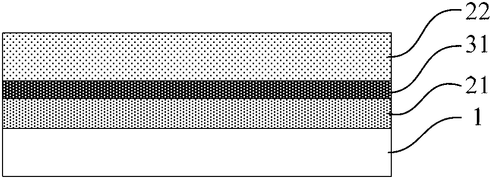
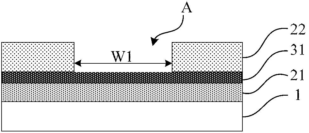
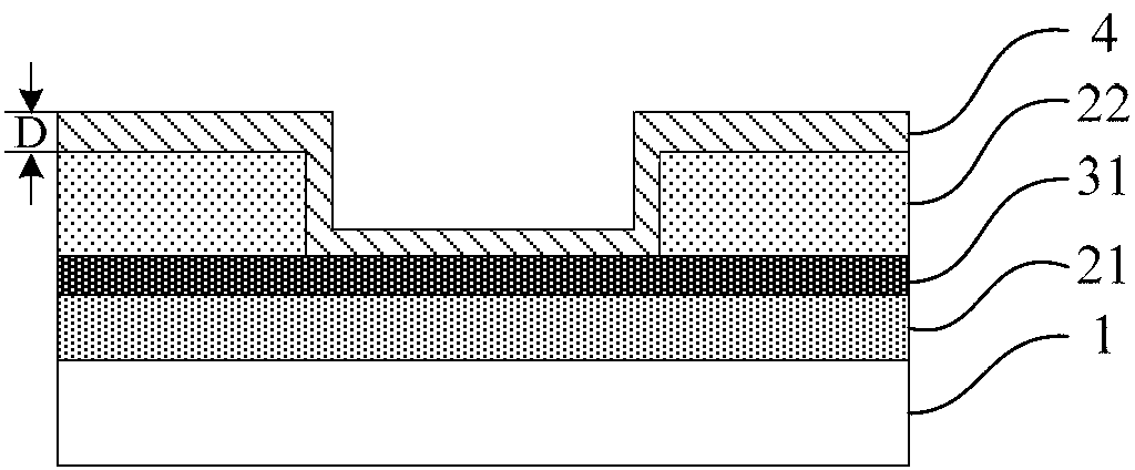
[0080] see Figure 1G , the present invention provides a phase change memory cell, comprising at least: Si substrate 1, first dielectric material layer 21, lower electrode layer 31, second dielectric material layer 22, phase change material layer 4, third dielectric material layer 23 And the upper electrode layer 32.

[0081] The first dielectric material layer 21 is formed on the surface of the Si substrate; the lower electrode layer 31 is formed on the surface of the first dielectric material layer 21 .

[0082] The upper surfaces of the second dielectric material layer 22, the phase change material layer 4 and the third dielectric material layer 23 are all located on the same plane, and at the same time, the second dielectric material layer 22, the phase change material layer 4 and the third dielectric material layer The layers 23 are all formed on the lower electrode layer 31 and are in contact with the lower electrode layer 31 .

[0083] The phase-change material layer ...

Embodiment 2

[0116] Such as Figure 2D As shown, the present invention provides a phase-change memory cell, which at least includes: a Si substrate 1 , a second dielectric material layer 22 , an electrode pair 5 , a phase-change material layer 4 and a third dielectric material layer 23 . in, Figure 2D It is a schematic structural diagram of a phase change memory cell in this embodiment.

[0117] The second dielectric material layer 22 is formed on the surface of the Si substrate 1 . Wherein, the second dielectric material layer 22 is an oxygen-free semiconductor dielectric material, at least including any one of gallium nitride, germanium nitride or silicon nitride. In this embodiment it is silicon nitride.

[0118] The electrode pair 5 is formed on the surface of the second dielectric material layer 22 , and two electrodes in the electrode pair 5 have a first distance and are separated from each other. Wherein, the range of the first distance is 10-100 nanometers, in this embodiment,...


PUM

PropertyMeasurementUnit
Thicknessaaaaaaaaaa
Thicknessaaaaaaaaaa
Thickness rangeaaaaaaaaaa

Abstract

The invention provides a phase change storage unit and a preparing method of the phase change storage unit. A phase change material layer with the thickness identical to the size of a single unit cell or a plurality of unit cells is adopted, interfacial characteristics are fundamentally expressed by the phase change material layer, volume material characteristics are weakened, so that the two-dimensional phase change storage unit which stores information through interface resistance change is prepared, and the two-dimensional phase change storage unit is high in density, low in power consumption and high in speed. The phase change material layer is thin and a small number of shortages exist on an interface of the phase change material layer, so that the operation power consumption of the phase change storage unit is reduced, and the operation time of the phase change storage unit is shortened, damage to a phase change material in every operation process is reduced, the element segregation effect of the material in every operation process is decreased, the maximum operability number of times of the phase change storage unit is increased, and therefore the capacity of circulating operation number of times of a device can be increased. Further, a graphene electrode used in the phase change storage unit has the advantages of being fast in signal response, large in mechanical strength, small in energy loss and the like. Meanwhile, the phase change storage unit is compatible with a novel CMOS.

Description

technical field [0001] The invention belongs to the technical field of microelectronics and relates to a phase-change memory unit and a preparation method thereof, in particular to a two-dimensional phase-change memory unit with high density, low power consumption and high speed and a preparation method thereof. Background technique [0002] Phase Change Random Access Memory (PCRAM) uses operating signals to generate Joule heat to operate phase change materials to make them transition between different phases, thereby reflecting the difference in high and low resistance values ​​and completing the storage of information. Phase-change memory is considered to be the most promising next-generation non-volatile memory due to its fast operation speed, good data retention, strong cycle operation capability, compatibility with traditional CMOS processes, and ability to maintain its operational performance in small sizes. one of the memory. [0003] Phase change material is the inf...

Claims


Application Information

Patent Timeline
IPC IPC(8): H01L45/00
CPCH10N70/823H10N70/8265H10N70/8413H10N70/231H10N70/023H10N70/8828H10N70/063H10N70/841H10N70/884
Inventor 宋志棠任堃饶峰宋三年陈邦明
Owner SHANGHAI INST OF MICROSYSTEM & INFORMATION TECH CHINESE ACAD OF SCI
Why Eureka
Try Eureka