Organic-inorganic hybrid solar cell with passivated organic thin film and preparation method thereof

A technology of solar cells and organic thin films, applied in circuits, photovoltaic power generation, electrical components, etc., to reduce surface defects, enhance charge separation and transmission capacity, and improve photoelectric conversion performance and stability.

Active Publication Date: 2013-10-09
SUZHOU INAINK ELECTRONICS MATERIALS CO LTD
View PDF6 Cites 15 Cited by
  • Summary
  • Abstract
  • Description
  • Claims
  • Application Information

AI Technical Summary

Problems solved by technology

Studies have shown that in the passivation method of methylated silicon surface, the dangling bonds on the silicon surface cannot be completely covered by methyl groups, and the surface recombination rate of the methylated passivated silicon sur

Method used


Image

  • Organic-inorganic hybrid solar cell with passivated organic thin film and preparation method thereof
  • Organic-inorganic hybrid solar cell with passivated organic thin film and preparation method thereof
  • Organic-inorganic hybrid solar cell with passivated organic thin film and preparation method thereof

Examples


Embodiment 1

[0039]Commercialized n-type single crystal silicon wafers (100) are used with a thickness of 420 microns and a resistivity of 0.9-1.3 ohm cm. The n-type silicon wafers are cleaned and placed in a glove box for alkylation treatment. Immerse the silicon substrate in a saturated phosphorus pentachloride chlorobenzene solution, react at about 110°C for 30 minutes, then wash it twice with chlorobenzene solution and tetrahydrofuran solution respectively, and then dip the cleaned silicon substrate in methylmagnesium chloride ( CH 3 MgCl) in tetrahydrofuran solution (1M), react at 80°C for 8h, and finally soak in dilute hydrochloric acid solution for 40min, blow dry with nitrogen gun, and set aside.

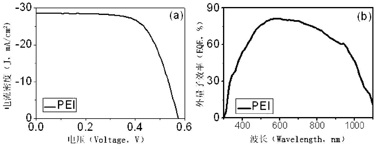
[0040] Using 2-methoxyethanol as solvent, PEI solutions with different concentrations were prepared. Then PEI solutions with different concentrations were spin-coated on the silicon substrate at a speed of 5000 rpm for 1 min, followed by annealing at 100° C. for 10 min to form PEI organ...

example 2

[0045] Commercialized n-type single crystal silicon wafers (100) are used with a thickness of 420 microns and a resistivity of 0.9-1.3 ohm cm. The n-type silicon wafers are cleaned and placed in a glove box for alkylation treatment. Immerse the silicon substrate in a saturated phosphorus pentachloride chlorobenzene solution, react at about 110°C for 30 minutes, then wash it twice with chlorobenzene solution and tetrahydrofuran solution respectively, and then dip the cleaned silicon substrate in methylmagnesium chloride ( CH 3 MgCl) in tetrahydrofuran solution (1M), react at 80°C for 8h, and finally soak in dilute hydrochloric acid solution for 40min, blow dry with nitrogen gun, and set aside.

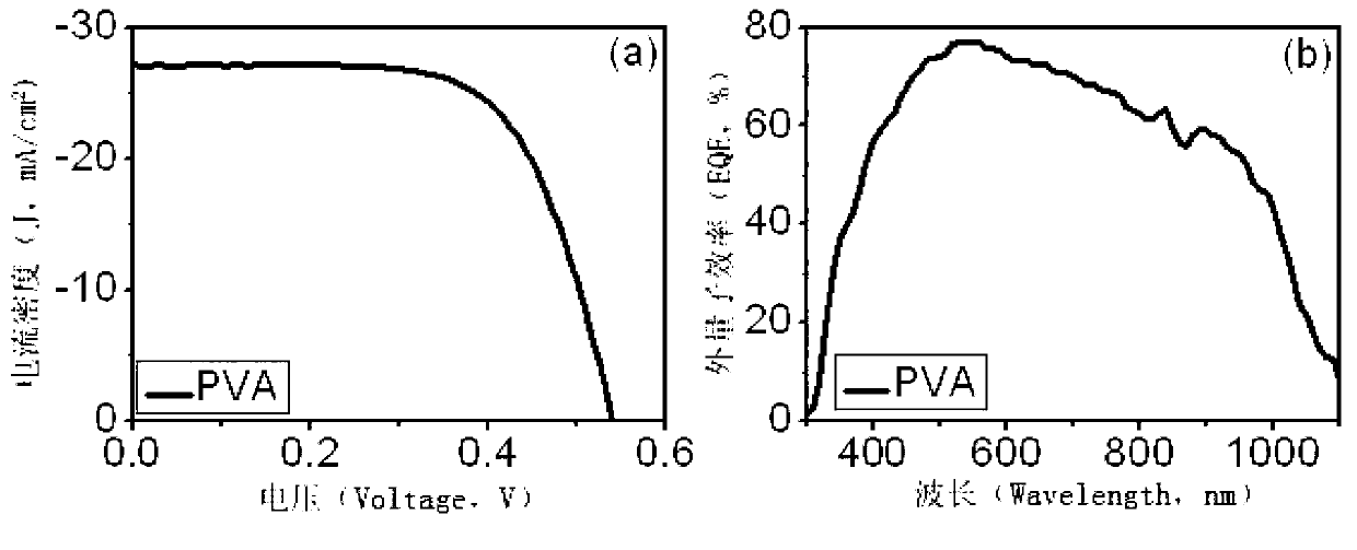
[0046] Using deionized water as solvent, PVA solutions with different concentrations were prepared. Then spin-coat PVA solutions with different concentrations on the silicon substrate at a speed of 5000 rpm for 1 min, and then anneal at 100° C. for 10 min to form PVA organic film passi...

example 3

[0051] Commercialized n-type single crystal silicon wafers (100) are used with a thickness of 420 microns and a resistivity of 0.9-1.3 ohm cm. The n-type silicon wafers are cleaned and placed in a glove box for alkylation treatment. Immerse the silicon substrate in a saturated phosphorus pentachloride chlorobenzene solution, react at about 110°C for 30 minutes, then wash it twice with chlorobenzene solution and tetrahydrofuran solution respectively, and then dip the cleaned silicon substrate in methylmagnesium chloride ( CH 3 MgCl) in tetrahydrofuran solution (1M), react at 80°C for 8h, and finally soak in dilute hydrochloric acid solution for 40min, blow dry with nitrogen gun, and set aside.

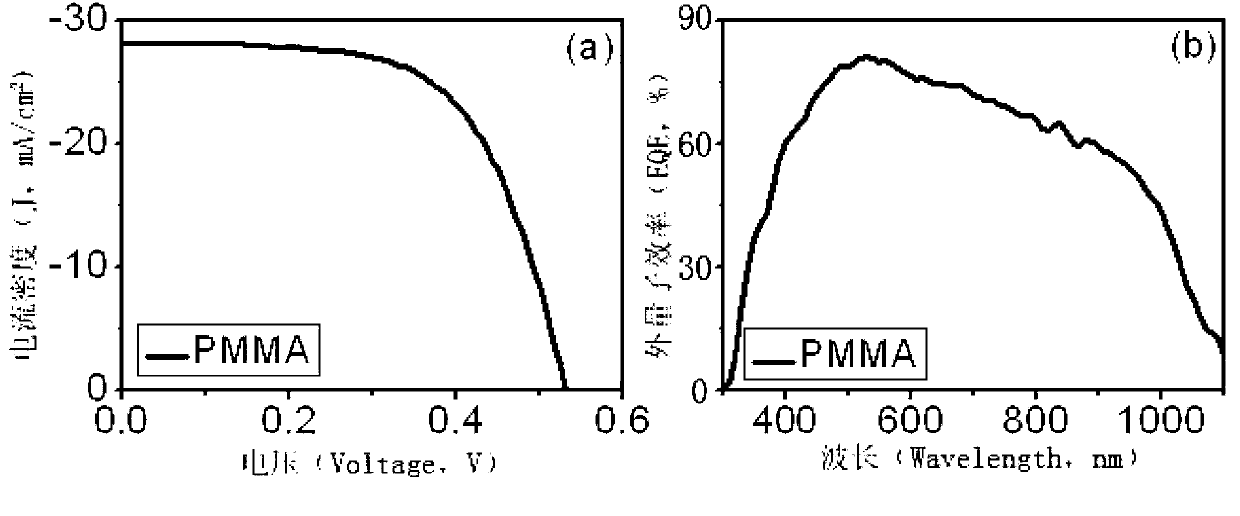
[0052] Using toluene as solvent, PMMA solutions with different concentrations were prepared. Then spin-coat PMMA solutions with different concentrations on the silicon substrate at a speed of 4000 rpm for 1 min, and then anneal at 100° C. for 10 min to form PMMA organic film passivatio...


PUM

PropertyMeasurementUnit
Thicknessaaaaaaaaaa
Thicknessaaaaaaaaaa
Thicknessaaaaaaaaaa

Abstract

The invention discloses an organic-inorganic hybrid solar cell with a passivated organic thin film. The solar cell mainly comprises a front face silver fence electrode, an organic electricity conducting thin film, an n-type monocrystalline silicon substrate processed through alkylate, and a back face aluminum electrode or an indium gallium alloy electrode, and further comprises an organic thin film passivated layer covering the front face of the n-type monocrystalline silicon substrate processed through alkylate. The organic electricity conducting thin film is covered on the organic thin film passivated layer. The front face silver fence electrode is arranged on the organic electricity conducting thin film. The back face aluminum electrode or the indium gallium alloy electrode is covered on the back face of the n-type monocrystalline silicon substrate processed through alkylate and forms ohmic contact with the back face of the n-type monocrystalline silicon substrate processed through alkylate. According to the method, a single rotating coating method is used to form various organic passivated films on the silicon surface, and the organic-inorganic hybrid heterojunction solar cell which is based on the organic thin film passivated layer and reaches 11% in photoelectric converting rate is formed.

Description

technical field [0001] The invention relates to a novel heterojunction solar cell and its preparation, in particular to an organic-inorganic hybrid solar cell based on an organic film passivated silicon surface and a preparation method thereof. Background technique [0002] Because monocrystalline silicon has the advantages of abundant resources, non-toxicity, and wide-band light absorption range, it has become the main raw material for commercial solar cell production. The photoelectric conversion efficiency of monocrystalline silicon solar cells is very high, but high-purity silicon, high-temperature annealing process (about 1000 ° C) and complicated manufacturing process are required in its production, resulting in high cost of this type of cell. With the development of the solar cell industry, organic solar cells are expected to reduce their production costs due to their advantages such as cheap materials, low annealing temperature, and simple manufacturing process. Howe...

Claims


Application Information

Patent Timeline
IPC IPC(8): H01L51/42H01L51/44H01L51/46H01L51/48
CPCY02E10/549
Inventor 孙宝全刘东宋涛申小娟张付特
Owner SUZHOU INAINK ELECTRONICS MATERIALS CO LTD
Why Eureka
Try Eureka