Polycrystalline silicon ingots and preparation method thereof, polycrystalline silicon chips and polycrystalline silicon ingot casting crucible

A technology of polycrystalline silicon ingots and polycrystalline silicon wafers, which is applied to the growth of polycrystalline materials, chemical instruments and methods, and crystal growth. It can solve the problems of reducing the crystal quality of the crucible wall area, the leakage probability of cells with induced defects, and the long diffusion distance of impurities. It is suitable for large-scale production, the preparation method is simple and convenient, and the effect of improving the quality of silicon ingots

Active Publication Date: 2013-10-23
JIANGXI SAI WEI LDK SOLAR HI TECH CO LTD
View PDF4 Cites 24 Cited by
  • Summary
  • Abstract
  • Description
  • Claims
  • Application Information

AI Technical Summary

Problems solved by technology

[0003] In the existing polycrystalline ingot casting process mentioned above, polycrystalline nucleation on the side wall of the quartz crucible has the following disadvantages: 1) During the melting and directional solidification process of the silicon material, the side wall of the crucible has a high temperature due to its proximity to the heater. Impurities such as nitrogen oxides and silicon oxides generated by the chemical reaction between the side wall and the inner wall silicon nitride coating are easy to melt and enter the crystal during the crystal growth stage, and are easy to form inclusions, induce defects and battery leakage probability; 2 ) The crystals on the side of the crucible nucleate in the form of dendrites to form grains with a certain crystal orientation, and the grains are larger, the grain boundaries are less, and the diffusion distance of impurities in the grains is longer, thereby reducing the number of crystals near the crucible wall. quality

Method used


Image

  • Polycrystalline silicon ingots and preparation method thereof, polycrystalline silicon chips and polycrystalline silicon ingot casting crucible
  • Polycrystalline silicon ingots and preparation method thereof, polycrystalline silicon chips and polycrystalline silicon ingot casting crucible
  • Polycrystalline silicon ingots and preparation method thereof, polycrystalline silicon chips and polycrystalline silicon ingot casting crucible

Examples


Embodiment 1

[0038] The preparation method of polycrystalline silicon ingot comprises the following steps:

[0039] (1) After coating the silicon nitride layer on the inner wall of the crucible, spray silicon powder with a purity of 99.99% on the silicon nitride layer inside the side wall of the crucible to obtain a barrier layer with a thickness of 3 mm; the particle size of the silicon powder 1~8μm;

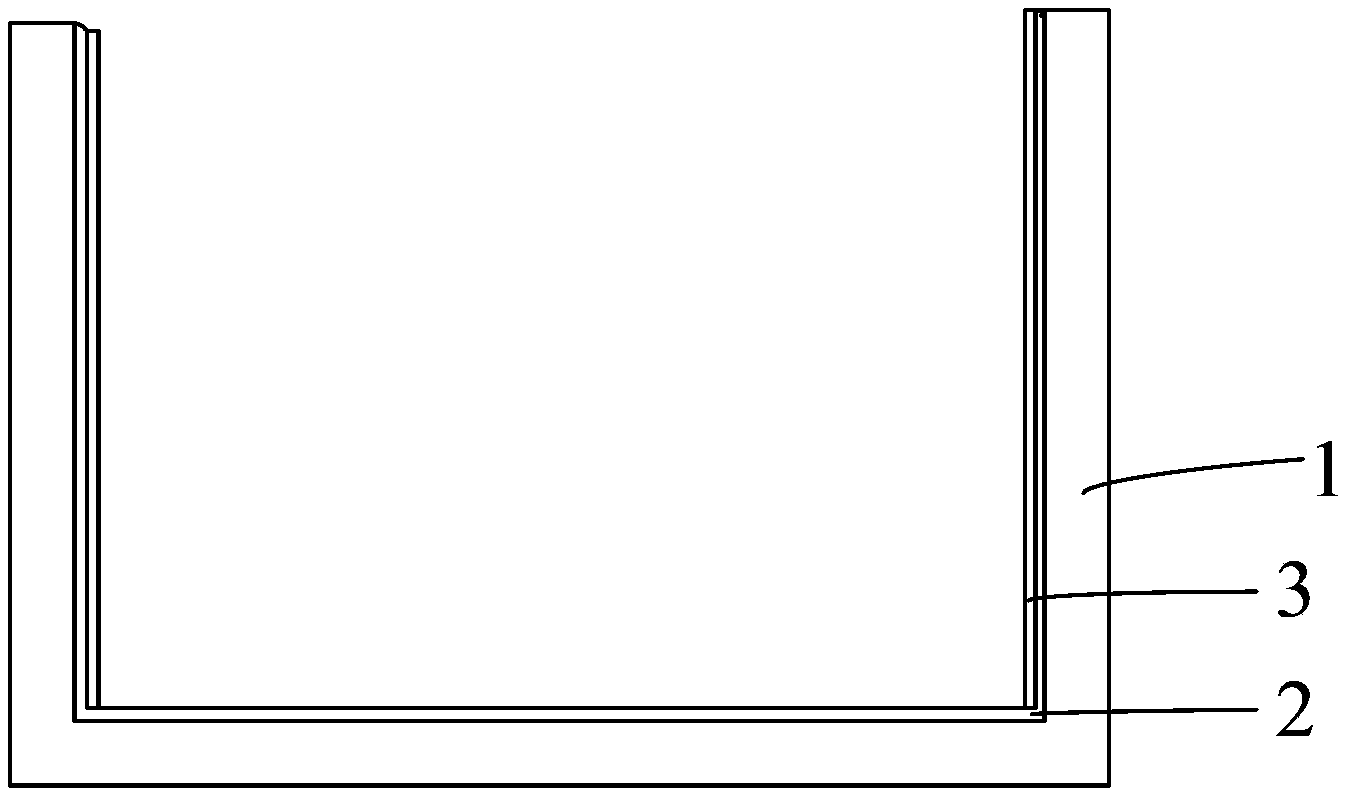
[0040] figure 1 A schematic diagram of a crucible for polysilicon ingots prepared in an embodiment of the present invention. Wherein, 1 is the crucible body, 2 is the silicon nitride layer, and 3 is the barrier layer provided on the side wall of the crucible.

[0041] (2) Then set molten silicon material in the crucible;

[0042] Wherein, setting the silicon material in molten state is as follows: 530 kg of solid silicon material is loaded in the crucible, and the crucible is heated to 1560° C. to melt the solid silicon material.

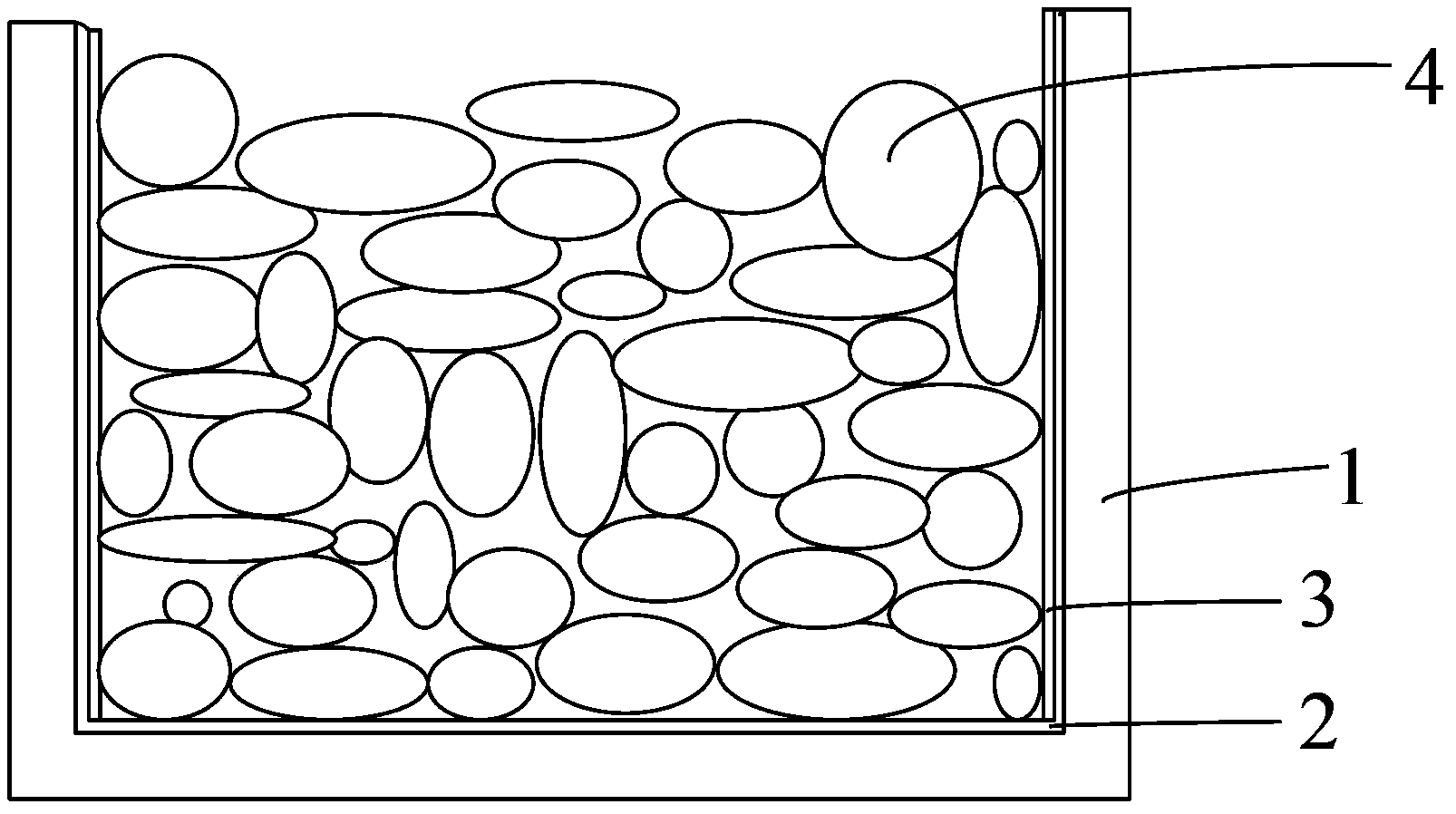
[0043] figure 2 It is a schematic diagram of the prep...

Embodiment 2

[0049] The preparation method of polycrystalline silicon ingot comprises the following steps:

[0050](1) After coating the silicon nitride layer on the inner wall of the crucible, spray quartz powder with a purity of 99.9999% on the silicon nitride layer inside the side wall of the crucible to obtain a barrier layer with a thickness of 2 mm; the particle size of the quartz powder 1~20μm;

[0051] (2) Then set molten silicon material in the crucible;

[0052] Wherein, setting the silicon material in molten state is as follows: 530 kg of solid silicon material is loaded in the crucible, and the crucible is heated to 1560° C. to melt the solid silicon material.

[0053] (3) Controlling the temperature in the crucible to gradually rise in a direction perpendicular to the bottom of the crucible to form a temperature gradient, so that the silicon material in the molten state begins to crystallize; after all crystallization is completed, annealing and cooling is performed to obtain...

Embodiment 3

[0058] The preparation method of polycrystalline silicon ingot comprises the following steps:

[0059] (1) Spray quartz powder with a purity of 99.9999% on the inner wall of the crucible to prepare a barrier layer with a thickness of 5 mm; the particle size of the quartz powder is 1-5 μm, and then spray a silicon nitride coating on the quartz powder barrier layer;

[0060] (2) Then set molten silicon material in the crucible;

[0061] Among them, setting the silicon material in the molten state is: heating 530 kg of solid silicon material in another crucible to 1560 ° C to obtain molten silicon material, and pouring the molten silicon material into the step (1). In the crucible of layers;

[0062] (3) Controlling the temperature in the crucible to gradually rise in a direction perpendicular to the bottom of the crucible to form a temperature gradient, so that the silicon material in the molten state begins to crystallize; after all crystallization is completed, annealing and ...


PUM

PropertyMeasurementUnit
thicknessaaaaaaaaaa
particle diameteraaaaaaaaaa

Abstract

The invention provides a preparation method of polycrystalline silicon ingots. The preparation method comprises the following steps: before or after the inner wall of a crucible is sprayed with a silicon nitride layer, a barrier layer is arranged on the inner side of the side wall of the crucible, wherein the barrier layer is a silicon powder coating layer, or a quartz powder coating layer, or a silicon powder and quartz powder mixed coating layer, and purities of silicon powder and quartz powder are above 99.99%; then a molten silicon material is arranged in the crucible; temperature in the crucible is controlled to increase gradually, along a direction which is perpendicular to the bottom of the crucible and is upward, to form a temperature gradient to make the molten silicon material to begin crystallization; and after the crystallization is finished, and the polycrystalline silicon ingots are obtained through annealing and cooling . The invention also provides the high quality polycrystalline silicon ingots obtained by the preparation method, and polycrystalline silicon chips prepared from the polycrystalline silicon ingots and the polycrystalline silicon ingot casting crucible. The polycrystalline silicon ingots prepared by the preparation method are characterized in that crystalline grains near areas of crucible wall are smaller, uniform and regular, dislocation density is low, and impurities is less.

Description

technical field [0001] The invention relates to the field of polycrystalline silicon ingots, in particular to polycrystalline silicon ingots and a preparation method thereof, polycrystalline silicon slices and a crucible for polycrystalline silicon ingots. Background technique [0002] At present, the preparation method of polycrystalline silicon ingot mainly adopts the directional solidification system method (DSS for short) furnace crystal growth technology provided by GT Solar. This method usually puts silicon material into a quartz crucible whose inner wall is sprayed with silicon nitride coating. After the silicon material is completely melted, the temperature at the bottom of the crucible is gradually reduced, so that the silicon melt continues to crystallize from the bottom of the crucible until it solidifies completely. The quality of crystals in the area near the crucible is lower than that in the central area of ​​the ingot. [0003] In the existing polycrystallin...

Claims


Application Information

Patent Timeline
Patent Type & Authority Applications(China)
IPC IPC(8): C30B28/06C30B29/06C30B33/00
Inventor 雷琦胡动力何亮张学日董一迪
Owner JIANGXI SAI WEI LDK SOLAR HI TECH CO LTD
Why Eureka
Try Eureka