

Surface-enhanced Raman substrate, preparation method and application thereof
A surface-enhanced Raman and substrate technology, applied in Raman scattering, material excitation analysis, etc., can solve the problems of poor enhancement effect, difficult preservation and uniform distribution of colloidal particles, and achieve excellent Raman activity, which is beneficial to industrial production. , the effect of easy availability of raw materials
- Summary
- Abstract
- Description
- Claims
- Application Information
AI Technical Summary
Problems solved by technology
Method used
Image

Examples
Embodiment 1
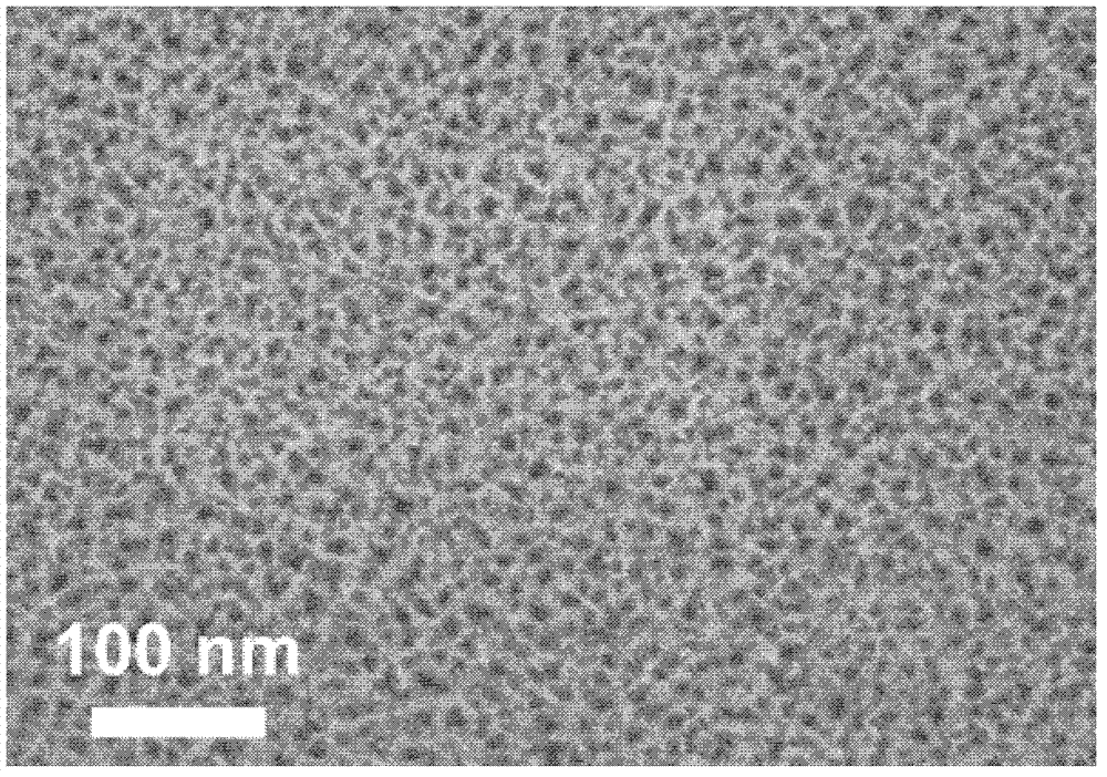
[0066] Use boron-doped P-type silicon wafers (that is, P-type B dope) for electrolysis and immersion plating. The specific steps are as follows:
[0067] (1) Preparation of the silicon wafer: place the silicon wafer in H with a volume ratio of 7:3 2 SO 4 (98% by weight) and H 2 o 2 (30% by weight) in the mixed solution, wash at 120° C. for 1 hour, then rinse with deionized water;
[0068] (2) Preparation of porous silicon substrate: The electrolytic cell with the upper and lower openings, the O-shaped plastic gasket and the silicon wafer prepared in step (1) are closely attached from top to bottom to form an open electrolytic cell with the silicon wafer as the bottom. , then add electrolytic solution in this exposed electrolytic cell, this electrolytic solution is made up of ethanol and hydrofluoric acid, and the volume ratio of ethanol and hydrofluoric acid (40% by weight aqueous solution) is 1: 3;
[0069] Wherein, make the aluminum foil close to the silicon chip for co...
Embodiment 2
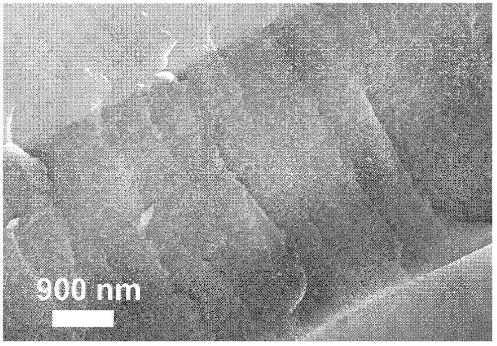
[0073] Use boron-doped P-type silicon wafers (that is, P-type B dope) for electrolysis and immersion plating. The specific steps are as follows:
[0074] (1) Preparation of the silicon wafer: place the silicon wafer in H with a volume ratio of 7:3 2 SO 4 (98% by weight) and H 2 o 2 (30% by weight) in the mixed solution, wash at 120° C. for 1 hour, then rinse with deionized water;
[0075] (2) Preparation of porous silicon substrate: The electrolytic cell with the upper and lower openings, the O-shaped plastic gasket and the silicon wafer prepared in step (1) are closely attached from top to bottom to form an open electrolytic cell with the silicon wafer as the bottom. , then add electrolytic solution in this exposed electrolytic cell, this electrolytic solution is made up of ethanol and hydrofluoric acid, and the volume ratio of ethanol and hydrofluoric acid (40% by weight aqueous solution) is 1: 3;
[0076] Wherein, make the aluminum foil close to the silicon chip for co...
Embodiment 3
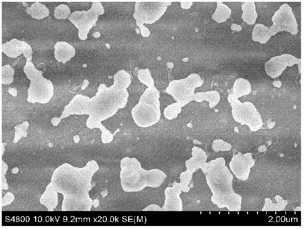
[0080] Use boron-doped P-type silicon wafers (that is, P-type B dope) for electrolysis and immersion plating. The specific steps are as follows:
[0081] (1) Preparation of the silicon wafer: place the silicon wafer in H with a volume ratio of 7:3 2 SO 4 (98% by weight) and H 2 o 2 (30% by weight) in the mixed solution, wash at 120° C. for 1 hour, then rinse with deionized water;
[0082] (2) Preparation of porous silicon substrate: The electrolytic cell with the upper and lower openings, the O-shaped plastic gasket and the silicon wafer prepared in step (1) are closely attached from top to bottom to form an open electrolytic cell with the silicon wafer as the bottom. , then add electrolytic solution in this exposed electrolytic cell, this electrolytic solution is made up of ethanol and hydrofluoric acid, and the volume ratio of ethanol and hydrofluoric acid (40% by weight aqueous solution) is 1: 3;
[0083] Wherein, make the aluminum foil close to the silicon chip for co...
PUM
| Property | Measurement | Unit |
|---|---|---|
| particle size | aaaaa | aaaaa |
| pore size | aaaaa | aaaaa |
| thickness | aaaaa | aaaaa |
Abstract
Description
Claims
Application Information