

Noble metal ceramic film and preparation method thereof
A ceramic thin film and precious metal technology, applied in the field of design and preparation of new metal ceramic thin film materials, can solve the problems of surface plasmon resonance absorption effect, change the electronic structure of Ag metal, low melting point of alloy, etc., and achieve excellent anti-oxidation performance and cost. Inexpensive, inexpensive effects
- Summary
- Abstract
- Description
- Claims
- Application Information
AI Technical Summary
Problems solved by technology
Method used
Image

Examples
Embodiment 1
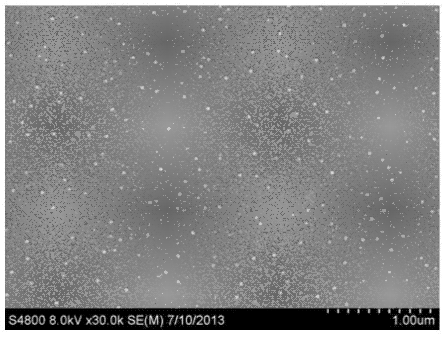
[0045] Place the quartz wafer and (100) single crystal silicon wafer to be plated in the deposition chamber, pre-evacuate, and the background vacuum is 4×10 -4 Pa, heat the quartz sheet and (100) single crystal silicon sheet to make the temperature 150°C, and at the same time pass Ar gas to raise the pressure of the vacuum chamber to 0.45Pa, keep it warm for 30min for desorption, and remove the impurities physically adsorbed on the surface of the substrate , which is conducive to improving the bonding force between the film and the substrate; then close the introduction of Ar gas, and re-pump the deposition chamber to 2×10 -4 Pa, and Ar gas was introduced again to increase the pressure of the deposition chamber to 0.45Pa; turn on the RF bias of the substrate, set its power to 100W and glow, sputter for 10min, and further clean the surface of the substrate; turn off the cleaning bias and Turn on Al 2 o 3 For the RF drive power supply of the target, adjust its power to 120W, p...
Embodiment 2
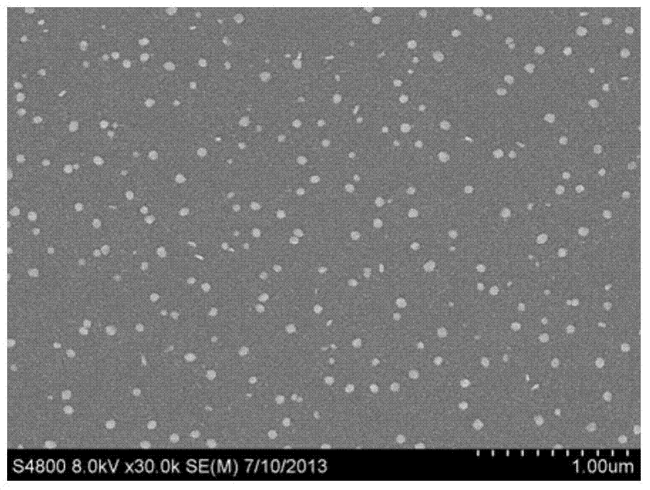
[0051] Place the quartz plate to be plated in the deposition chamber, pre-evacuate, and the background vacuum is 3.6×10 -4 Pa, heat the quartz substrate to a temperature of 150°C, and at the same time pass in Ar gas to increase the pressure of the deposition chamber to 0.45 Pa, keep it warm for 30 minutes for desorption, and remove physically adsorbed impurities on the surface of the substrate, which is beneficial to enhance the film and substrate The binding force between the sheets; then close the flow of Ar gas, and re-pump the deposition chamber to 1.8×10 -4 Pa, and Ar gas was introduced again to increase the pressure of the deposition chamber to 0.45Pa; turn on the RF bias of the substrate, set its power to 100W and glow, sputter for 10min, and further clean the surface of the substrate; turn off the cleaning bias and Turn on Al 2 o 3 For the RF drive power supply of the target, adjust its power to 120W, pre-sputter for 60 minutes, turn on the drive power of the Ag targ...
Embodiment 3
[0053] Place the quartz substrate to be plated in the deposition chamber, pre-evacuate, and the background vacuum is 3.4×10 -4 Pa, heat the quartz substrate to a temperature of 150°C, and at the same time pass in Ar gas to increase the pressure of the vacuum chamber to 0.45Pa, keep it warm for 30min for desorption, and remove physically adsorbed impurities on the surface of the substrate, which is beneficial to enhance the film and substrate The binding force between the sheets; then close the introduction of Ar gas, and re-pump the vacuum chamber to 1.6×10 -4 Pa, and re-introduce Ar gas to raise the pressure of the vacuum chamber to 0.45Pa again; turn on the substrate RF bias, set its power to 100W and glow, sputter for 10min, and further clean the substrate surface; turn off the cleaning bias and Turn on Al 2 o 3 For the RF drive power supply of the target, adjust its power to 120W, pre-sputter for 60 minutes, turn on the drive power of the Ag target and Ti target at the s...
PUM
 Abstract
Description
Claims
Application Information