Insulating material forming composition for electronic elements, insulating material for electronic elements, electronic element, and thin film transistor

A technology for electronic components and insulating materials, which is applied in the field of compositions for forming insulating materials for electronic components, can solve the problems of inability to form components, high leakage current density, and inability to withstand the coating process, and achieve low leakage current density and low leakage The effect of current density

Inactive Publication Date: 2013-10-23
IDEMITSU KOSAN CO LTD
View PDF6 Cites 3 Cited by
  • Summary
  • Abstract
  • Description
  • Claims
  • Application Information

AI Technical Summary

Problems solved by technology

[0008] However, there is room for improvement of conventionally known polymer insulators
First, the types of polymer insulators that can be coated and formed are limited
In addition, even polymer insulators that can be coated and formed into films usually cannot withstand the subsequent coating process, such as the formation of the semiconductor layer of bottom gate (bottom gate) TFT, the formation of conductive layers such as electrodes, and the formation of TFT after TFT formation. The conditions used for the formation of the protective layer, etc. (for example, the type of solvent applied), and the element cannot be formed
[0009] Second, polymer insulators are often low heat-resistant substances, especially acrylic polymer insulating films represented by polymethyl methacrylate (PMMA), which generally cannot withstand such as the formation of organic EL display devices, Process temperature used in the formation of organic EL elements after TFT formation, etc. Process temperature of subsequent processes after TFT formation
[0010] Third, the leakage current density of existing polymer insulators is relatively high (usually higher than 1×10 at 2MV / cm -7 A / cm 2 ), so good TFT characteristics cannot be obtained
However, due to the lack of cross-linking functionality, when other layers are further formed by a solution process after film formation, dissolution, etc., may occur in the subsequent film formation process, and may not be able to withstand the formation of devices
[0014] As a method for solving these problems, cross-linked polymer insulators such as Patent Document 2, Patent Document 3, and Non-Patent Document 4 have been reported, but the monomer structure of the present invention has not yet been disclosed

Method used


Image

  • Insulating material forming composition for electronic elements, insulating material for electronic elements, electronic element, and thin film transistor
  • Insulating material forming composition for electronic elements, insulating material for electronic elements, electronic element, and thin film transistor
  • Insulating material forming composition for electronic elements, insulating material for electronic elements, electronic element, and thin film transistor

Examples


Embodiment 1

[0269] 0.4 g (colorless transparent liquid) of 1,3-adamantane dimethanol diacrylate (compound (1)) (manufactured by Idemitsu Kosan Co., Ltd.) represented by the following structural formula, benzoin as a polymerization initiator 0.04 g of isobutyl ether and 4 g of MEK as a solvent were mixed to obtain a composition for forming an insulating material (film) having a solid content concentration of 10% by mass.

[0270] [chemical formula 28]

[0271]

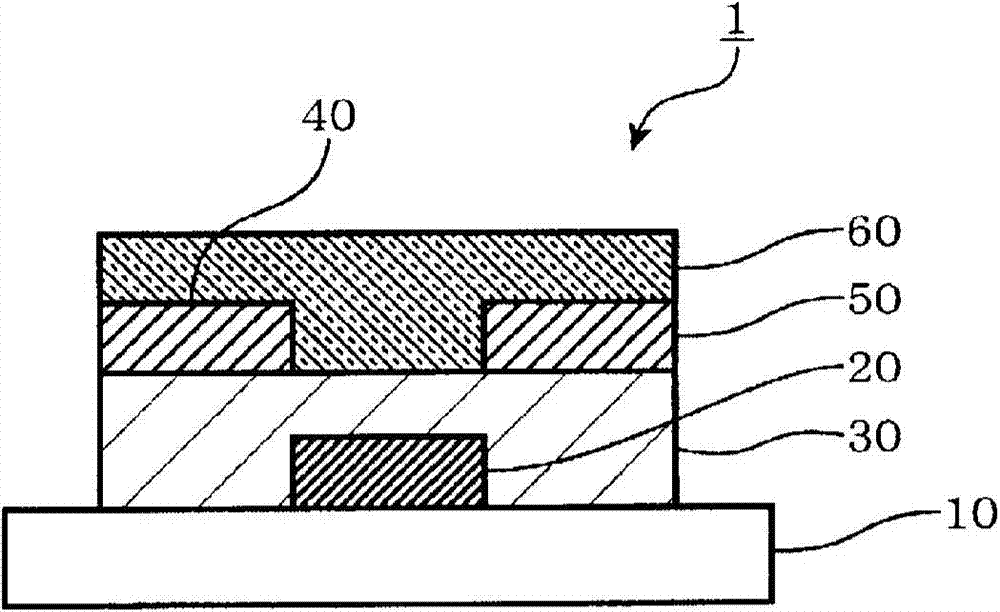
[0272] Use glass with a size of 25 × 20 × 1.1mm as a substrate, form an ITO film with a thickness of 100 nm on the substrate, and use photolithography to pattern it to make a transparent gate electrode (hereinafter, the substrate with the ITO film is referred to as transparent. supporting substrate). Clean the transparent support substrate with isopropanol ultrasonically for 5 minutes, then clean it with pure water for 5 minutes, then use isopropanol ultrasonically for 5 minutes, then blow dry it. 2 air to dry. Then, finally,...

Embodiment 2

[0291] Using a composition containing the following compound (2) instead of compound (1), the same operation as in Example 1 was performed to form an insulator layer, and the same operation as in Example 1 was performed to evaluate the insulator layer. Compound (2) was produced by the method described in Examples 1 and 2 of WO2007 / 020901 pamphlet. The results are shown in Table 1. Then, the same operation as in Example 1 was performed to fabricate a thin film transistor and evaluate it. The results are shown in Table 2.

[0292] [chemical formula 29]

[0293]

Embodiment 3

[0295] Using a composition containing the following compound (3) (agent manufactured by Aldrich Corporation) instead of compound (1), the same operation as in Example 1 was used to form an insulator layer, and the same operation as in Example 1 was performed for the insulator layer. evaluate. The results are shown in Table 1.

[0296] [chemical formula 30]

[0297]


PUM

PropertyMeasurementUnit
thicknessaaaaaaaaaa
particle diameteraaaaaaaaaa

Abstract

An insulting material forming composition for electronic elements, which contains, as a polymerizable component, a monomer that has two or more (meth)acrylic moieties and a polycyclic alicyclic structure.

Description

technical field [0001] The present invention relates to a composition for forming an insulating material for electronic components and an electronic component using the composition. Background technique [0002] Insulation materials used for interlayer insulation are essential materials in electronic components with switching functions such as thin film transistors (TFTs), organic EL elements, and liquid crystal cells. [0003] Thin film transistors, which are typical electronic elements, are widely used as switching elements of display devices such as liquid crystal display devices and organic EL display devices. [0004] Conventionally, this TFT has been produced using amorphous silicon or polycrystalline silicon, but there are CVD (Chemical Vapor Deposition, chemical vapor deposition) devices used in the production of TFTs using silicon are very expensive, and large-scale display devices such as TFTs are used. This will be accompanied by problems such as a substantial in...

Claims


Application Information

Patent Timeline
Patent Type & Authority Applications(China)
IPC IPC(8): H01L21/312C08F20/20C08F20/28H01L29/786H01L51/05H01L51/30
CPCH01L29/408H01L51/052C08F20/28H01B3/447H10K10/471
Inventor 栗原直树齐藤雅俊
Owner IDEMITSU KOSAN CO LTD
Why Eureka
Try Eureka