Manufacturing method of ultramicropore broadband flexible micro-perforated plate

A technology of micro-perforated plate and manufacturing method, which is applied in the field of vibration reduction and noise reduction, can solve the problems of not suitable, lack of flexibility of micro-perforated plate, small deformation, etc., and achieve the effect of high processing precision, compact structure and small volume

Inactive Publication Date: 2013-11-13
HEFEI INSTITUTES OF PHYSICAL SCIENCE - CHINESE ACAD OF SCI
View PDF5 Cites 12 Cited by
  • Summary
  • Abstract
  • Description
  • Claims
  • Application Information

AI Technical Summary

Problems solved by technology

Micro-perforated plates processed with these materials lack flexibility and have little deformation,

Method used


Image

  • Manufacturing method of ultramicropore broadband flexible micro-perforated plate
  • Manufacturing method of ultramicropore broadband flexible micro-perforated plate
  • Manufacturing method of ultramicropore broadband flexible micro-perforated plate

Examples


Example Embodiment

[0016] Example 1 Using MEMS technology to process a single crystal silicon template with a cylindrical array diameter of 50um

[0017] (1) Use square glass with a side length of 10cm to make a lithography plate, and the distribution density of the opaque circular pattern on the lithography plate is 5×10 7 Pcs / m2;

[0018] (2) Choose a single-sided polished silicon wafer with a diameter of 4 inches and a crystal orientation of (100) with a thickness of 500 microns, and then chemically clean the single-crystal polished silicon wafer, and then dry it;

[0019] (3) A 600nm thick silicon dioxide film and a 300nm thick metal aluminum film are sequentially grown and deposited on the polished surface of the monocrystalline silicon wafer;

[0020] (4) Spin-coating a layer of photoresist with a thickness of 2 microns on the metal aluminum film;

[0021] (5) After the steps of exposure, development, fixing, hardening, etc., the cylindrical array pattern on the photoresist plate is transferred...

Example Embodiment

[0026] Example 2 Using the above cylindrical array template to make a flexible micro-perforated plate with an ultra-micro aperture of 50um

[0027] (1) Carry out chemical treatment to reduce the surface energy of the above-mentioned processed monocrystalline silicon cylindrical array template, clean and dry;

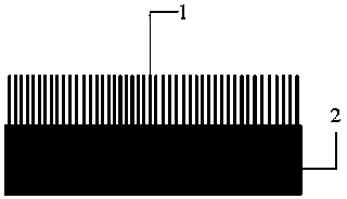
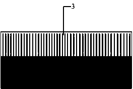
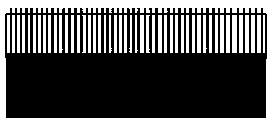
[0028] (2) The two-component polyether polyurethane, which is a flexible material with a certain viscosity and configured as a liquid, is deposited on the surface of the cylindrical array template by spin coating or casting; see figure 2 , The gaps of the cylindrical array are filled with flexible material two-component polyether polyurethane, and the flexible material 3 completely contains the cylindrical array 2;

[0029] (3) Place the above-mentioned template with flexible material 3 in an oven set at a temperature of 80 degrees Celsius for about 30 minutes to completely cure the two-component polyether polyurethane flexible material deposited on the surface of the cylindri...

Example Embodiment

[0032] Example 3 Using LIGA technology to process templates with a cylindrical array diameter of 100um

[0033] (1) Use Au as the absorber to make an X-ray lithography plate so that the distribution density of the opaque circular pattern on the lithography plate is 6×10 6 Pcs / square meter.

[0034] (2) Chemical cleaning of single-crystal polished silicon wafers and post-drying treatment; single-crystal silicon wafers can be single-sided polished or double-sided polished silicon wafers with any crystal orientation and any resistivity. The diameter can be 2 inches to 4 inches. In this example, a single-sided polished silicon wafer with a diameter of 4 inches and a crystal orientation of (100) is selected, and the thickness is 500 microns;

[0035] (3) On the polished surface of the single crystal silicon wafer, a layer of conductive material metal nickel film is grown and deposited by the radio frequency sputtering process, the thickness of which is 300 nanometers;

[0036] (4) Spi...


PUM

PropertyMeasurementUnit
Diameteraaaaaaaaaa
Heightaaaaaaaaaa
Diameteraaaaaaaaaa

Abstract

The invention relates to the manufacturing of sound absorbing material, and particularly to an ultramicropore broadband flexible micro-perforated plate. The manufacturing process comprises the following steps: first using micro mechanical processing method to produce a cylindrical array template formed by silicon, ceramic, metal and glass or plexiglass material, wherein the diameter of each cylinder is between 10 and 500 microns, the height of each cylinder is between 10 and 500 microns, and the distribution density of the cylinders is between 104 and 1010 cylinders per square meter; depositing liquid polymeric material on a substrate of the cylindrical array template with spin coating or casting techniques, and allowing the upper end surface of the cylinders to be exposed, wherein the polymeric material is polyurethane, polyimide, silica gel or the like; then carrying out solidification processing on the polymeric material deposited on the surface of the cylindrical array template; and finally removing the cylindrical array template to obtain a finished flexible micro-perforated plate. The method is high in processing speed, low in cost, compact in structure, and small in size, with consistent apertures, wide sound absorbing bands, and good flexibility, and thus can satisfy noise reduction needs of devices in different shapes.

Description

technical field [0001] The invention relates to the technical field of vibration reduction and noise reduction, and also relates to the production technology of sound-absorbing materials. In particular, it relates to a method for manufacturing a flexible ultra-microporous broadband micro-perforated plate. Background technique [0002] The micro-perforated board sound absorbing body is an important sound-absorbing material. It is durable, clean and pollution-free, and can be used in harsh environments such as high temperature, high humidity and high-speed airflow. It is an ideal green sound-absorbing material in the 21st century. Now it has It is widely used in various fields of noise control. [0003] An important part of the micro-perforated plate sound absorber is a micro-perforated plate, that is, a thin plate with a large number of micro-holes on the plate surface. Its sound absorption mechanism is that a large number of micropores and the cavity behind the thin plate ...

Claims


Application Information

Patent Timeline
IPC IPC(8): B81C1/00
Inventor 孔德义钱玉洁刘淑梅王焕钦朱利凯孙少明李子博李山山殷世平吴志会
Owner HEFEI INSTITUTES OF PHYSICAL SCIENCE - CHINESE ACAD OF SCI
Why Eureka
Try Eureka