
Oxide sintered compact and sputtering target

一种氧化物、烧结体的技术,应用在溅射镀覆、半导体/固态器件制造、离子注入镀覆等方向,能够解决不均匀、电阻率高等问题,达到生产率提高、削减原料成本的效果

Active Publication Date: 2013-11-27
KOBELCO RES INST
View PDF8 Cites 8 Cited by
  • Summary
  • Abstract
  • Description
  • Claims
  • Application Information

AI Technical Summary

Problems solved by technology

However, when ZTO-based is produced by the conventional atmospheric pressure sintering method, the resistivity is high and tends to become non-uniform, so abnormal discharge may occur during sputtering

Method used


Image

  • Oxide sintered compact and sputtering target
  • Oxide sintered compact and sputtering target
  • Oxide sintered compact and sputtering target

Examples


experiment example 1

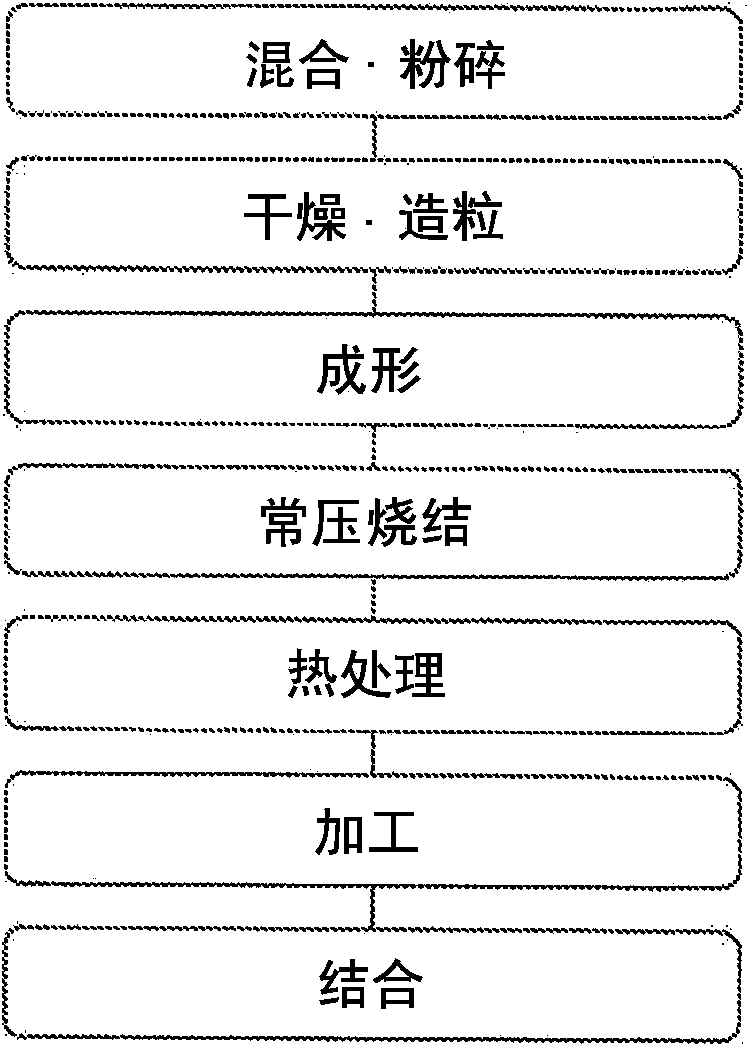
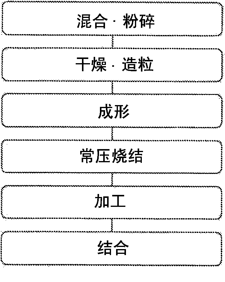
[0074] Zinc oxide powder (JIS 1 type) with a purity of 99.99%, tin oxide powder with a purity of 99.99%, and alumina powder with a purity of 99.99% are blended at a ratio of [Zn]:[Sn]:[Al]=73.9:24.6:1.5, Mix with a nylon ball mill for 20 hours. The Zn ratio and the Sn ratio are shown in Table 1 for reference. The Al ratio was 0.015. Next, the mixed powder obtained in the above process is dried and granulated, and pressed with a mold at a molding pressure of 0.5 tonf / cm 2 After preforming, use CIP with a forming pressure of 3tonf / cm 2 Do the main shaping.

[0075] The compacts thus obtained were held at 1500° C. for 7 hours under normal pressure as shown in Table 1, and sintered. Oxygen is introduced into the sintering furnace, and sintering is carried out in an oxygen environment. Next, it was introduced into a heat treatment furnace, and heat treatment was performed at 1200° C. for 10 hours. Nitrogen gas is introduced into the heat treatment furnace, and heat treatment ...

experiment example 2

[0081] Zinc oxide powder (JIS 1 type) with a purity of 99.99%, tin oxide powder with a purity of 99.99%, and tantalum oxide powder with a purity of 99.99% are mixed in a ratio of [Zn]:[Sn]:[Ta]=73.9:24.6:1.5, After sintering at 1550° C. for 5 hours, heat treatment was performed at 1150° C. for 14 hours, and the oxide sintered body of Experimental Example 2 (Ta ratio = 0.015) was obtained in the same manner as in Experimental Example 1 above.

[0082] The relative density and resistivity of the oxide sintered body of Experimental Example 2 obtained in this way were measured in the same manner as in Experimental Example 1 above. As a result, the relative density was 90% or more and the resistivity was 0.10Ω·cm or less, which were good results.

[0083] Next, DC (direct current) magnetron sputtering was performed on the above-mentioned oxide sintered body in the same manner as in the above-mentioned Experimental Example 1. As a result, no abnormal discharge (arc) was observed, and...

experiment example 3

[0087] Zinc oxide powder (JIS 1 type) with a purity of 99.99%, tin oxide powder with a purity of 99.99%, and indium oxide powder with a purity of 99.99% are mixed at a ratio of [Zn]:[Sn]:[In]=45.0:45.0:10.0, The oxide sintered body of Experimental Example 3 (In ratio = 0.10) was obtained in the same manner as in Experimental Example 1 above except that it was sintered at 1550° C. for 5 hours (without heat treatment).

[0088] The relative density and resistivity of the oxide sintered body of Experimental Example 3 thus obtained were measured in the same manner as in Experimental Example 1 above. As a result, good results were obtained with a relative density of 90% or more and a resistivity of 0.10Ω·cm or less.

[0089] Next, DC (direct current) magnetron sputtering was performed on the above-mentioned oxide sintered body in the same manner as in the above-mentioned Experimental Example 1. As a result, no abnormal discharge (arc) was observed, and stable discharge was confirmed...


PUM

PropertyMeasurementUnit
electrical resistivityaaaaaaaaaa
purityaaaaaaaaaa
electrical resistivityaaaaaaaaaa

Abstract

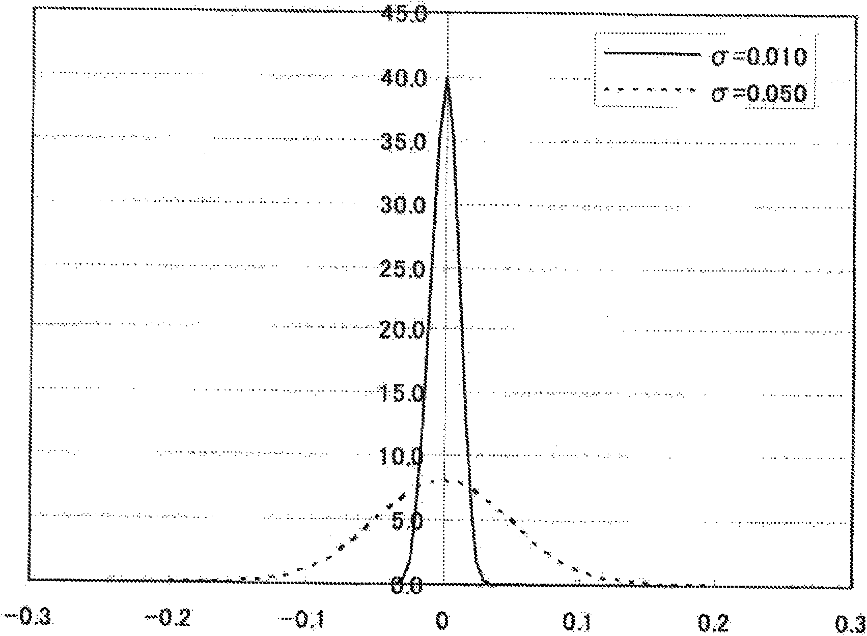
Provided are an oxide sintered compact and a sputtering target that are ideal for the production of an oxide semiconductor film for a display device. The oxide sintered compact and sputtering target that are provided have both high conductivity and high relative density, are capable of forming an oxide semiconductor film having a high carrier mobility, and in particular, have excellent direct-current discharge stability in that long-term, stable discharge is possible, even when used by the direct-current sputtering method. The oxide sintered compact of the invention is an oxide sintered compact obtained by mixing and sintering zinc oxide, tin oxide, and an oxide of at least one metal (M metal) selected from the group consisting of Al, Hf, Ni, Si, Ga, In, and Ta. When the in-plane specific resistance and the specific resistance in the direction of depth are approximated by Gaussian distribution, the distribution coefficient s of the specific resistance is 0.02 or less.

Description

technical field [0001] The present invention relates to an oxide sintered body and a sputtering target used when forming an oxide semiconductor thin film of a thin film transistor (TFT) used in a display device such as a liquid crystal display or an organic EL display by a sputtering method. Background technique [0002] The amorphous (amorphous) oxide semiconductor used in TFT has higher carrier mobility and a larger optical band gap than the general-purpose amorphous silicon (a-Si), and can be formed at a low temperature, so , It is expected to be applied to next-generation displays that require large-scale, high-resolution, and high-speed drives, and resin substrates with low heat resistance. When forming the above-mentioned oxide semiconductor (film), it is preferable to use a sputtering method of sputtering a sputtering target made of the same material as the film. Thin films formed by sputtering are superior to those formed by ion plating, vacuum deposition, and elect...

Claims


Application Information

Patent Timeline
Patent Type & Authority Applications(China)
IPC IPC(8): C04B35/453C04B35/457C23C14/08C23C14/34H01L21/363
CPCC04B2235/3251C04B35/457C04B35/453H01L21/02631C04B2235/3284H01L21/02554C04B2235/3293C04B2235/3217H01L21/02565C23C14/3414C04B2235/3286C04B2235/3244C23C14/08C23C14/086C23C14/34H01L21/34
Inventor 后藤裕史岩崎祐纪
Owner KOBELCO RES INST
Learn More