Partial SOI (silicon on insulator) super junction high-voltage power semiconductor device

A power semiconductor, high-voltage technology, applied in the direction of semiconductor devices, electrical components, circuits, etc., can solve the problem of device withstand voltage and on-resistance contradiction, can not completely improve the electric field distribution of the device, etc. voltage, the effect of increasing the breakdown voltage

Inactive Publication Date: 2013-12-04
UNIV OF ELECTRONICS SCI & TECH OF CHINA +1
View PDF5 Cites 5 Cited by
  • Summary
  • Abstract
  • Description
  • Claims
  • Application Information

AI Technical Summary

Problems solved by technology

[0006] However, this structure cannot completely improve the electric field distribution in the device body, and there is still a contradiction between the device withstand voltage and on-resistance

Method used


Image

  • Partial SOI (silicon on insulator) super junction high-voltage power semiconductor device
  • Partial SOI (silicon on insulator) super junction high-voltage power semiconductor device
  • Partial SOI (silicon on insulator) super junction high-voltage power semiconductor device

Examples


Embodiment Construction

[0022] Below in conjunction with accompanying drawing, the technical scheme of the present invention is described in detail:

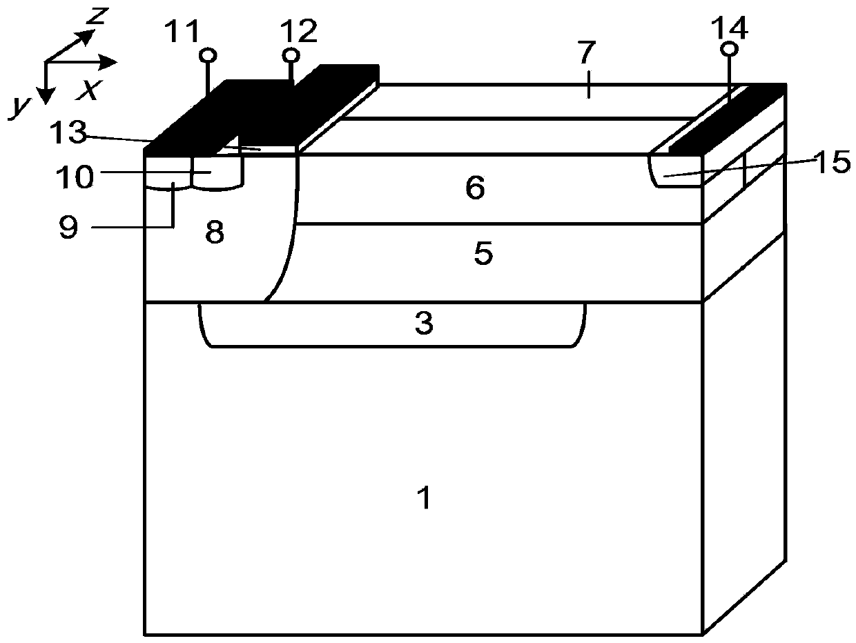
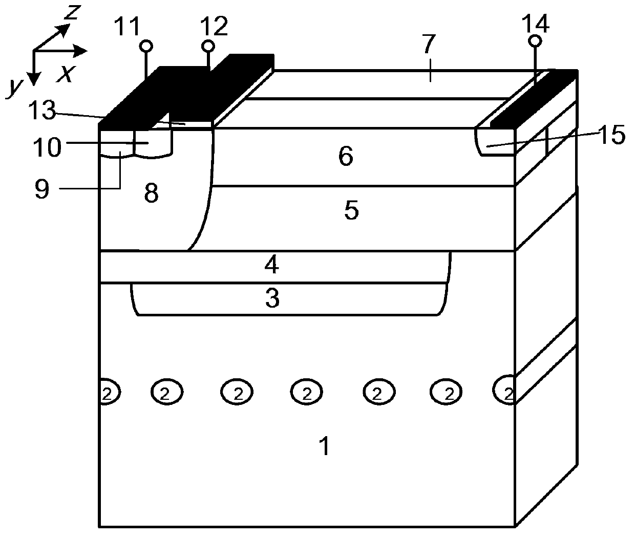
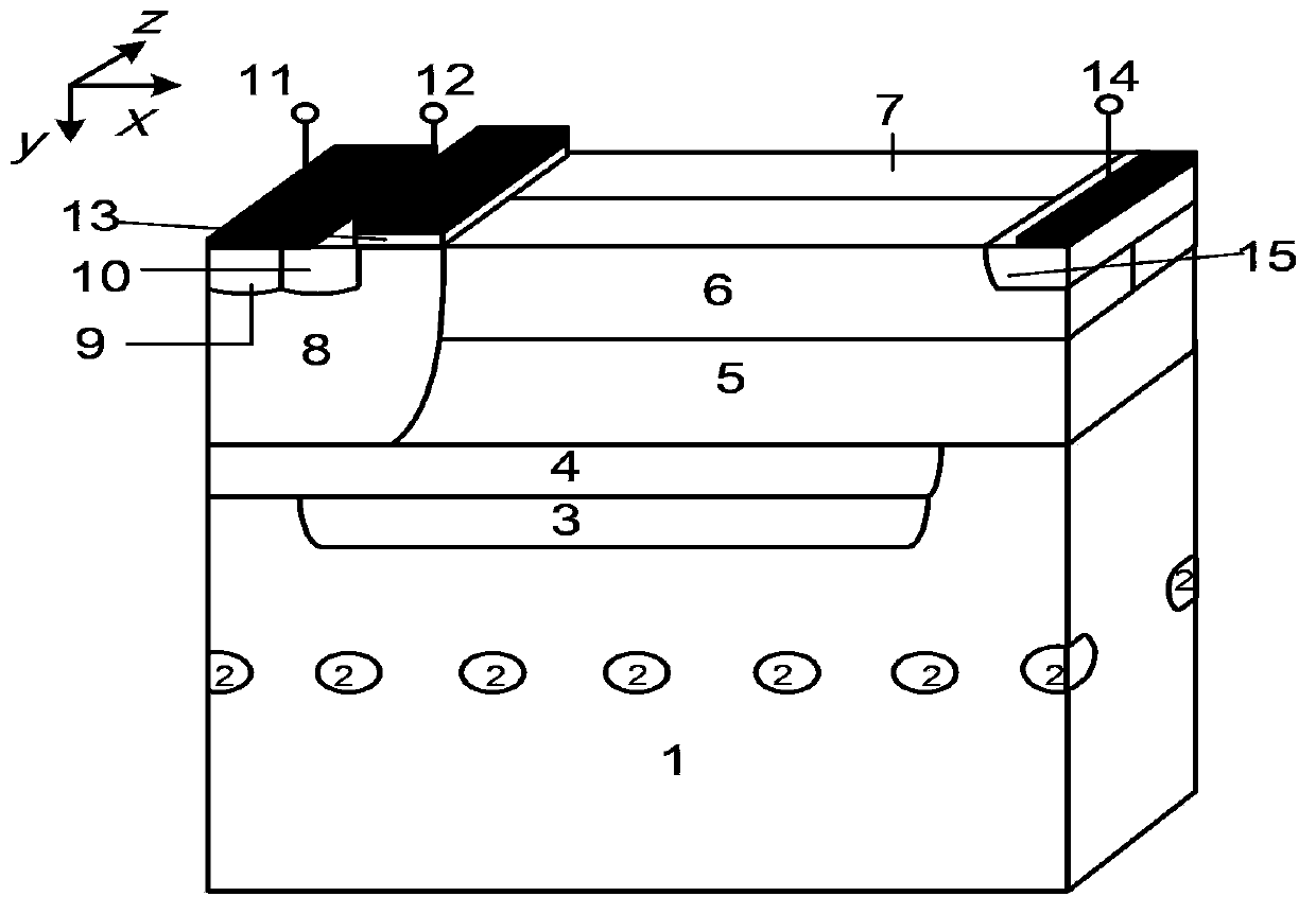
[0023] The present invention optimizes the specific on-resistance and breakdown voltage of the device by introducing heavily doped N+ islands 2 into the substrate 1 of some SOI superjunction power semiconductor devices, and introducing a P-type electric field shielding layer 4 on the buried oxide layer 3 .

[0024] The specific structure is as figure 2 As shown, it includes a P-type substrate 1, a buried oxide layer 3 in the substrate, a P-type electric field shielding layer 4, an N-type buffer 5, a P-type strip 6, an N-type strip 7, a P-type body region 8, and a P-type Heavily doped body contact region 9, N-type heavily doped source region 10, metal source electrode 11, polysilicon gate electrode 12, gate oxide layer 13, metal drain electrode 14, N-type heavily doped drain region 15; the buried oxygen The layer 3 is located in the P-type substrate ...


PUM


Abstract

The invention relates to semiconductor technology, in particular to a partial SOI (silicon on insulator) super junction high-voltage power semiconductor device. The partial SOI super junction high-voltage power semiconductor device is characterized by comprising a plurality of N+ pads and a P-type electric field shielding layer, the N+ pads are uniformly embedded into a P-type substrate, the P-type electric field shielding layer is arranged in the P-type substrate, the upper surface of the P-type electric field shielding layer is connected with a P-type body area and the lower surface of an N-type buffer area close to a source end, and the lower surface of the P-type electric field shielding layer is connected with the upper surface of a buried oxide layer. The partial SOI super junction high-voltage power semiconductor device has the advantages that the doping concentration of a drift region is increased by changing electric field distribution, the voltage resistance of the device is improved, on resistance is reduced, the area of the device is decreased, and cost is reduced. The invention is particularly applicable to the partial SOI super junction high-voltage power semiconductor device.

Description

technical field [0001] The invention relates to semiconductor technology, in particular to a partial SOI super-junction high-voltage power semiconductor device. Background technique [0002] With the rapid development of information technology, power MOSFET devices have been widely used for their advantages of fast switching speed, no secondary breakdown, negative temperature coefficient and good thermal stability. In the design of power MOS devices, the relationship between the breakdown voltage BV (Breakdown Voltage) and the specific on-resistance Ron,sp is limited by the "silicon limit". Its structure breaks the theoretical limit of traditional power MOS devices, and has lower conduction losses while maintaining all the advantages of power MOS. [0003] Lateral Double-diffused MOSFET (LDMOS) is the core device of HVIC (High Voltage Integrated Circuit) and power integrated circuit PIC (Power Integrated Circuit). Its main feature is that a relatively long lightly doped dr...

Claims


Application Information

Patent Timeline
Patent Type & Authority Applications(China)
IPC IPC(8): H01L29/06H01L29/78
CPCH01L29/0634H01L29/1083H01L29/7816
Inventor 乔明蔡林希章文通胡利志张波
Owner UNIV OF ELECTRONICS SCI & TECH OF CHINA
Why Eureka
Try Eureka