Method for controlling size and distribution of metal surface micro-nanostructure

A micro-nano structure, metal surface technology, applied in metal processing equipment, manufacturing tools, welding equipment, etc., can solve problems such as increasing the cost of processing equipment, limiting the size of the focusing spot, and limiting the control of the grating period, and achieves a wide range of metal types. , The production process is simple, and the processing depth is large.

Active Publication Date: 2013-12-11
CHANGCHUN UNIV OF SCI & TECH
View PDF6 Cites 26 Cited by
  • Summary
  • Abstract
  • Description
  • Claims
  • Application Information

AI Technical Summary

Problems solved by technology

[0004] The laser can produce a submicron grating structure on the metal surface by the plasma wave resonance effect induced by the laser. The size of such a submicron grating structure depends on the wavelength of the incident laser. Since the adjustment of the laser wavelength is difficult, it is not easy to optimize the structure. Have good controllability
The use of femtosecond lasers to directly focus on metal processing will cause mass migration on the metal surface. A large number of spatters will make it difficult to apply short focusing lenses in industrial processing, and indirectly limit the optimization of the focus spot size, further limiting the grating period. control
Moreover, the technology of laser processing micro-nano structures on metal surfaces must ensure the size of the laser focus spot, which requires high precision of the focus system and increases the cost of processing equipment.

Method used


Image

  • Method for controlling size and distribution of metal surface micro-nanostructure
  • Method for controlling size and distribution of metal surface micro-nanostructure
  • Method for controlling size and distribution of metal surface micro-nanostructure

Examples


Embodiment 1

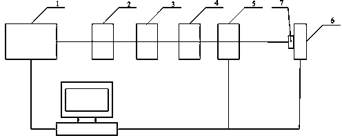
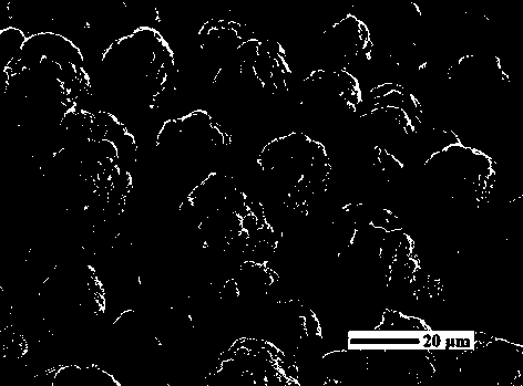
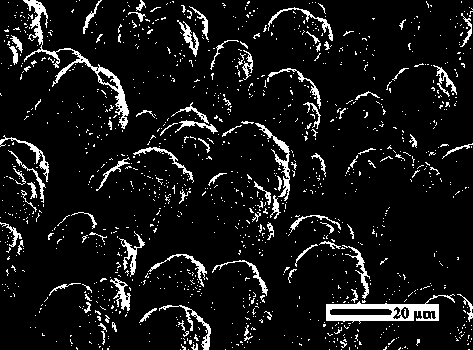
[0035] The metal sample in this embodiment is aluminum, and the aluminum sample is placed under the filament induced by the femtosecond pulse laser. The center wavelength of the femtosecond pulse laser selected in this example is 800nm, the repetition frequency is 1kHz, the pulse width is 50fs, and the horizontal line A polarized femtosecond laser with a single pulse energy of 3.5 mJ passes through a focusing lens with a focal length of 1 m to form a plasma filament about 11 cm in length. The sample is fixed on the three-dimensional translation stage, and the fixed direction of the translation stage is perpendicular to the plasma filament, so that the plasma filament can irradiate the surface of the metal sample vertically. The distance between the sample processing position and the focusing lens is 95cm. By moving the three-dimensional translation stage, the scanning speed is 5mm / s, change the scanning distance to 0.02mm-0.08mm, so as to control the distribution density and s...

Embodiment 2

[0037] The sample, laser parameters, and filamentation parameters used in this embodiment are the same as in Example 1. The sample is fixed on a three-dimensional translation platform, and the fixed direction of the translation platform makes the surface of the sample and the plasma filament be placed at an angle (90°, 75°, 60° , 45°), so that the plasma filament can be inclined to irradiate the surface of the metal sample, the distance between the sample processing position and the focusing lens is 95cm, the scanning speed of the translation stage is 4mm / s, and the scanning distance is 0.04mm. The angle between the plasma filament and the metal aluminum surface is used to control the pitch direction of the micro-nano structure on the metal aluminum surface, and the results are as follows Figure 4-7 shown.

Embodiment 3

[0039] The sample, laser parameters, and filamentation parameters used in this embodiment are the same as in Example 1. The plasma filaments induced by circularly polarized and linearly polarized lasers with different polarization directions control the morphology of the micro-nanostructures on the aluminum surface. The results are as follows Figure 8-9 shown.


PUM

PropertyMeasurementUnit
thicknessaaaaaaaaaa
thicknessaaaaaaaaaa
thicknessaaaaaaaaaa

Abstract

The invention discloses a method for controlling the size and distribution of a metal surface micro-nanostructure. In order to implement the invention, plasma filaments induced by ultrashort pulse laser with the pulse width of 15fs-5ps are utilized to directly irradiate a metal surface, by controlling the ultrashort pulse laser parameters and the scanning speed and scanning spacing to the metal surface of the filaments, control of the plasma filaments on the size and distribution of the metal surface induced micro-nanostructure is realized; by changing the incidence angle of the laser induced plasma filaments, the orientation of the micro-nanostructure is changed; the control on the shape of the micro-nanostructure is realized by changing the polarizing character of the laser. The invention provides a method used for designing parts such as a solar absorber in an optimized manner.

Description

technical field [0001] The invention relates to the field of laser micromachining and the preparation of micro-nano structures on metal surfaces, in particular to a control method for preparing micro-nano structures on metal surfaces by ultrashort pulse laser treatment. Background technique [0002] There are not many technologies for metal surface modification at present. With the development of micro-processing technology and the gradual maturity of its theory, more and more scientific workers have turned their attention to the preparation and research of micro-nano structures on metal surfaces. Through different means and methods Micro-nanostructures prepared on metal surfaces have potential applications in different fields, such as solar energy absorption, high-efficiency thermal radiation sources, thermal radiation conversion, and biological detectors. [0003] Electron beam or plasma etching can be used to prepare micro-nano structures on the metal surface, but the pro...

Claims


Application Information

Patent Timeline
Patent Type & Authority Applications(China)
IPC IPC(8): B23K26/00B23K26/06
Inventor 陶海岩林景全宋晓伟刁凌天郝作强
Owner CHANGCHUN UNIV OF SCI & TECH
Why Eureka
Try Eureka