Processing method of silicon micro resonator

A technology of silicon microresonator and processing method, which is applied in the field of sensors to achieve the effect of high pressure resistance effect and stability, and easy operation

Inactive Publication Date: 2013-12-11
NO 49 INST CHINESE ELECTRONICS SCI & TECH GRP
View PDF3 Cites 9 Cited by
  • Summary
  • Abstract
  • Description
  • Claims
  • Application Information

AI Technical Summary

Problems solved by technology

[0007] The purpose of the present invention is to solve the problems existing in the production

Method used


Image

  • Processing method of silicon micro resonator
  • Processing method of silicon micro resonator
  • Processing method of silicon micro resonator

Examples


specific Embodiment approach 1

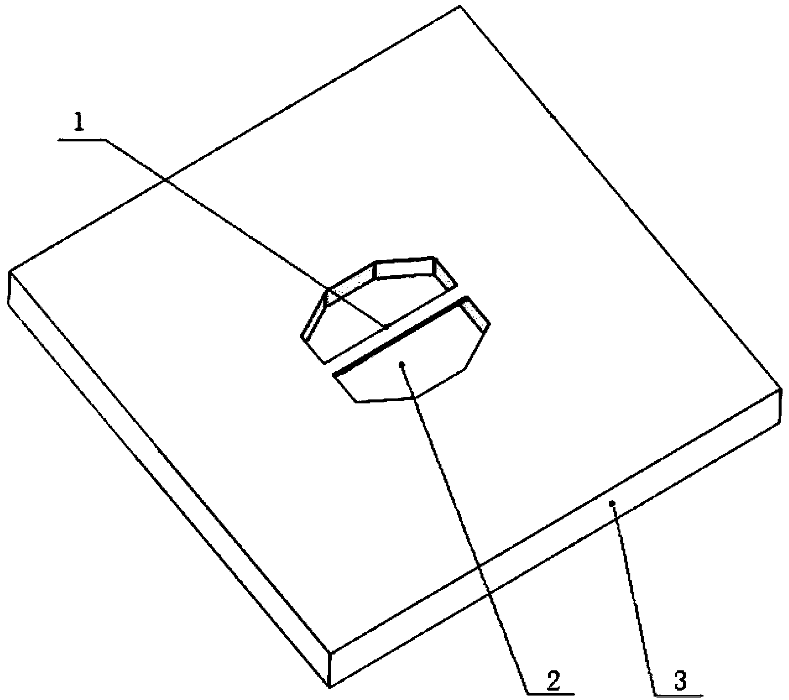
[0024] Specific implementation mode one: the following combination Figure 1 to Figure 8 Describe this embodiment mode, the processing method of silicon microresonator described in this embodiment mode, this method comprises the following steps:

[0025] Step 1. Select an N-type silicon wafer with a resistivity of 3Ω·cm~10Ω·cm as the silicon wafer to be processed, perform thermal oxidation treatment on the silicon wafer to be processed, form an oxide film on the upper and lower surfaces of the silicon wafer to be processed, and obtain Thermal oxidation treatment of silicon wafers;

[0026] Step 2: Etch the resonant beam structure pattern on the upper surface of the thermally oxidized silicon wafer by photolithography; then remove the oxide layer on both sides of the resonant beam by reactive ion etching process or wet etching process; The reactive ion etching process forms two deep grooves symmetrically on both sides of the resonant beam, and the depth of the deep grooves is...

specific Embodiment approach 2

[0035] Specific implementation mode two: this implementation mode further explains implementation mode one, and the process of etching the resonant beam structure pattern on the upper surface of the thermally oxidized silicon wafer by using the deep reactive ion etching process described in step two is:

[0036] Etching is carried out symmetrically on both sides of the structural pattern of the resonant beam to form two symmetrical deep grooves, the depth of the deep grooves is the thickness of the resonant beam, and the width of the interval between the two deep grooves is the width of the resonant beam.

[0037] The resonant beam is placed along the crystal direction, and the length of the resonant beam is its width more than double.

specific Embodiment approach 3

[0038] Embodiment 3: The manufacturing method of the resonator involved in this embodiment combines dry and wet etching processes of semiconductors, and utilizes the corrosion characteristics of silicon wafers. The resonator whose vibration frequency is 110kHz is taken as an example to illustrate its manufacturing method. The resonant beam is placed along the direction, with a thickness of 6 microns, a length and a width of 600 microns and 40 microns, respectively. It is located in a chamber with a depth of 20 microns. The length and width of the etched regions on both sides of the resonant beam are 600 microns and 200 microns, respectively.

[0039] The specific process steps are as follows:

[0040] (1) Use N-type silicon wafers with a resistivity of 3-10Ω·cm. thermal oxidation of silicon wafers (eg figure 2 , 3 shown);

[0041] (2) The pattern of the resonant beam structure is etched by deep reactive ion etching (DRIE). The resonant beams are arranged along the ...


PUM

PropertyMeasurementUnit
Resistivityaaaaaaaaaa

Abstract

The invention discloses a processing method of a silicon micro resonator, belongs to the field of sensors, and aims at solving the problems in an existing method for manufacturing a resonator. The method provided by the invention comprises the following steps: 1, performing thermal oxidation treatment on an N-type (111) silicon wafer (with the resistivity of 3Omega.cm-10Omega.cm) selected as a to-be-processed silicon wafer so as to obtain a thermal oxidation treatment type silicon wafer; 2, etching a resonance beam structure diagram on the upper surface of the thermal oxidation treatment type silicon wafer by adopting a photoetching technology; removing oxidation layers in areas at two sides of a resonance beam; meanwhile, forming two deep grooves symmetrically in the two sides of the resonance beam by utilizing a deep reaction ion etching technology; 3, covering passivation layers on side walls of the resonance beam; 4, etching passivation layers on the bottoms of the two deep grooves; 5, re-etching the bottoms of the two deep grooves again continuously by a certain depth; 6, corroding the silicon wafer by a TMAH (tetramethylammonium hydroxide) solution, and releasing the resonance beam; communicating the two deep grooves in two sides of the resonance beam to form a vibration chamber, and processing the silicon micro resonator.

Description

technical field [0001] The invention relates to a processing method of a silicon micro-resonator and belongs to the field of sensors. Background technique [0002] The long-term accuracy of the silicon microresonant pressure sensor can reach 0.01% FS. It is the silicon micro pressure sensor with the highest precision at present, and has strong anti-interference ability, stable performance, and the annual stability can reach 0.01%. Such sensors are urgently needed sensors in industrial control systems, atmospheric and cosmic data detection systems. The resonator is the core of this type of sensor. The core structure of the resonator is a resonant beam or a resonant membrane, and a vacuum cavity where the cantilever beam (membrane) is located. At present, the resonant beams (membranes) of resonators for such purposes are mainly produced by the following four methods, and these methods have their own shortcomings: [0003] (1) The resonator is completed by direct bonding of t...

Claims


Application Information

Patent Timeline
IPC IPC(8): G01L1/10G01L9/00B81B3/00
Inventor 王明伟金建东李玉玲田雷齐虹王永刚刘智辉
Owner NO 49 INST CHINESE ELECTRONICS SCI & TECH GRP
Why Eureka
Try Eureka