Method for forming inverted-pyramid porous surface nanometer texture on polycrystalline silicon and method for manufacturing short-wave reinforcing solar cell

An inverted pyramid-shaped, porous surface technology, applied in the direction of circuits, photovoltaic power generation, electrical components, etc., can solve problems such as limiting photoelectric conversion efficiency, achieve high short-wave spectral response, simple method and process, uniform and flat microstructure morphology Effect

Inactive Publication Date: 2013-12-18
SHANGHAI UNIV
View PDF2 Cites 54 Cited by
  • Summary
  • Abstract
  • Description
  • Claims
  • Application Information

AI Technical Summary

Problems solved by technology

However, even with optimally configured chemical etching methods and optical antireflection coatings, polycrystalline silicon solar cells still have a rather high surface reflectivity, thus limiting their photoelectric conversion efficiency

Method used


Image

  • Method for forming inverted-pyramid porous surface nanometer texture on polycrystalline silicon and method for manufacturing short-wave reinforcing solar cell
  • Method for forming inverted-pyramid porous surface nanometer texture on polycrystalline silicon and method for manufacturing short-wave reinforcing solar cell
  • Method for forming inverted-pyramid porous surface nanometer texture on polycrystalline silicon and method for manufacturing short-wave reinforcing solar cell

Examples


Embodiment 1

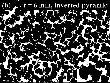
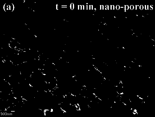
[0036] In this example, see Figure 1 to Figure 6 , a method for forming an inverted pyramid-shaped porous surface nanotexture on polysilicon, comprising the steps of:

[0037] (1) Use solar-grade polysilicon as the substrate material, which is P Type boron doping, the thickness is 200mm, the minority carrier lifetime is 2 ms, and the resistivity is 3 Ωcm; 3 h 6 O carry out 5 minutes ultrasonic cleaning to the silicon wafer as solar cell silicon substrate material, remove the organic residue on the surface of silicon wafer; 3 = (1:10), etch under the condition of 5°C, the reaction time is 3.5 minutes, so as to remove the mechanical damage layer on the surface of the silicon wafer, and its cross-sectional structure is shown in figure 1 , surface reflectance see Figure 4 ;

[0038] (2) Then, the silicon wafer was immersed in 0.004 mol / L HF and 0.32 mol / L AgNO 3 In an aqueous solution, react at room temperature for 15-20 seconds to deposit nano-silver particles on its surf...

Embodiment 2

[0043] This embodiment is basically the same as Embodiment 1, especially in that:

[0044] In this example, see Figure 5 and Image 6 , the nb-Si material sample was first immersed in dilute HF solution to remove its surface oxide layer, and then immediately immersed in 1% NaOH etching solution, the reaction time was 3 minutes, and the reaction temperature was room temperature. from Figure 5 It can be seen that in the wavelength range of 580-1000 nm, the surface reflectance of the IP-Si battery of this embodiment is lower than that of the nb-Si battery of Comparative Example 2. from Image 6 It can be seen that the nb-Si of Comparative Example 2 and the IP-Si battery of this embodiment EQE Curves and calculated photogenerated current densities J sc : respectively 24.8 mA / cm 2 and 31.6 mA / cm 2 , the photogenerated current density of the IP-Si battery of this embodiment is higher than that of the nb-Si battery of Comparative Example 2.

Embodiment 3

[0046] This embodiment is basically the same as Embodiment 1, especially in that:

[0047] In this example, see Figure 5 and Image 6 , the nb-Si material sample was first immersed in dilute HF solution to remove its surface oxide layer, and then immediately immersed in 1% NaOH etching solution, the reaction time was 9 minutes, and the reaction temperature was room temperature. from Figure 5 It can be seen that in the wavelength range of 580-1000 nm, the surface reflectance of the IP-Si battery of this embodiment is lower than that of the nb-Si battery of Comparative Example 2. from Image 6 It can be seen that the nb-Si of Comparative Example 2 and the IP-Si battery of this embodiment EQE Curves and calculated photogenerated current densities J sc : respectively 24.8 mA / cm 2 and 32.8mA / cm 2 , the photogenerated current density of the IP-Si battery of this embodiment is higher than that of the nb-Si battery of Comparative Example 2.


PUM

PropertyMeasurementUnit
thicknessaaaaaaaaaa
thicknessaaaaaaaaaa
thicknessaaaaaaaaaa

Abstract

The invention discloses a method for forming an inverted-pyramid porous surface nanometer texture on polycrystalline silicon and a method for manufacturing a short-wave reinforcing solar cell. The method for forming the inverted-pyramid porous surface nanometer texture on the polycrystalline silicon and the method for manufacturing the short-wave reinforcing solar cell are suitable for the technical field of solar photovoltaic batteries. By means of a metal catalytic chemical corrosion method, a nanometer porous surface structure is formed on the polycrystalline silicon through HF, AgNO3, H2O2, HNO3 and other solutions, then partial samples are placed in a NaOH corrosive liquid with the concentration of 0.1-1% for surface modification of a nanometer inverted pyramid, a nanometer inverted pyramid silicon structure is formed, and the micro structure appearance of the nanometer inverted pyramid silicon structure is even and smooth, so that service life of a few effective charge carriers is greatly prolonged, and ultimately, in the nanometer texture surface structure, by means of changes of the thickness of a silicon nitride layer in the solar cell manufacturing process, a nanometer inverted pyramid silicon solar photovoltaic cell which is low in surface reflection rate and high in short wave spectrum response is prepared. The method for forming the inverted-pyramid porous surface nanometer texture on the polycrystalline silicon and the method for manufacturing the short-wave reinforcing solar cell are simple in process, convenient to operate, low in cost and suitable for industrial production.

Description

technical field [0001] The invention relates to a method for surface treatment of silicon crystals and a subsequent method for preparing solar photovoltaic cells, in particular to a method for preparing nanoporous black silicon to form the surface texture of silicon crystals by using a metal-catalyzed chemical corrosion process and the method for silicon The invention discloses a method for preparing a crystalline solar cell, which is applied in the technical field of solar photovoltaic cells. Background technique [0002] The reflectivity of the untreated pristine polycrystalline silicon surface is very high, so the optical loss of polycrystalline silicon solar cells prepared directly from this material is quite large, which greatly limits the photoelectric conversion efficiency of the cell. In order to increase the absorptivity of incident light, the traditional anisotropic / isotropic chemical etching method is a relatively mature method in the industry, which can prepare m...

Claims


Application Information

Patent Timeline
Patent Type & Authority Applications(China)
IPC IPC(8): H01L31/0352H01L31/0236H01L31/18
CPCY02E10/50Y02P70/50
Inventor 马忠权石建伟徐飞
Owner SHANGHAI UNIV
Why Eureka
Try Eureka