Low temperature coefficient crystal boundary layer ceramic capacitor medium and preparation method thereof

A technology of ceramic capacitors and low temperature coefficient, applied in the field of low temperature coefficient grain boundary layer ceramic capacitor dielectric and its preparation, can solve problems such as low withstand voltage, and achieve the effects of high withstand voltage, cost reduction and low temperature coefficient

Inactive Publication Date: 2014-01-15
JIANGSU UNIV
View PDF6 Cites 9 Cited by
  • Summary
  • Abstract
  • Description
  • Claims
  • Application Information

AI Technical Summary

Problems solved by technology

[0002] With the rapid development and popularization of surface mount technology, the share of surface mount components (SMC) in electronic equipment has steadily increased; in 1997, the chip rate of electronic components in developed countries in the world has reached more than 70%, and the world average is 40%. % or more; in 2000, the chip rate of electronic components in the world reached 70%, and in 2002, the chip rate has exceeded 85%. With the increasingly urgent demand and the development trend of portability, miniaturization and multi-function of communication and information terminals, chip electronic components have entered a new era of comprehensive development; single-layer chip semiconductor ceramic materials are divided into surface layer type and grain boundary There are two types of layer types, which are characterized by small volume and large capacity. In addition, the grain boundary layer semiconductor ceramic material also has the advantages of good temperature characteristics, good frequency characteristics, and high operating frequency; currently, only AVX and JOHANSON are less than Ten companies can provide single-layer chip semiconductor ceramic materials. The global market demand for single-layer chip semiconductor ceramic material components is as high as 4.5 billion per year; With the increasingly urgent demand for high performance and high performance, semiconductor ceramic materials have been rapidly developed in terms of miniaturization, high dielectric constant, high precision and high frequency. Single-layer semiconductor ceramic materials are the development trend; general monolithic The sintering temperature of the grain boundary layer ceramic capacitor dielectric and the single-layer chip grain boundary layer ceramic capacitor dielectric is 1350~1430°C, and there are the following problems at the same time: either the withstand voltage is low, or the temperature coefficient is large, or the dielectric constant is low, The sintering process basically adopts the secondary sintering method, that is: first high-temperature reduction, then coating insulating oxide for oxidation heat treatment at medium temperature, the process is more complicated and the cost is higher; some use the coating method, the process is more complicated, and the raw materials Expensive and high cost; while the sintering temperature of the grain boundary layer ceramic capacitor medium of the present invention is about 1250°C, and a one-time sintering process is adopted at the same time, which can greatly reduce the cost of the grain boundary layer ceramic capacitor. lead and cadmium, capacitor ceramics do not pollute the environment during preparation and use; in addition, the dielectric constant of the capacitor ceramics of the present invention is high, which will improve the capacity of ceramic capacitors and miniaturization, which is in line with the development trend of ceramic capacitors, and will also Reduce the cost of ceramic capacitors, the grain boundary layer ceramic capacitors of the present invention have high dielectric withstand voltage, low temperature coefficient, and the temperature capacity characteristics meet the requirements of X7R, etc., which are conducive to expanding the use range and safety of grain boundary layer ceramic capacitors

Method used


Image

  • Low temperature coefficient crystal boundary layer ceramic capacitor medium and preparation method thereof

Examples


Embodiment Construction

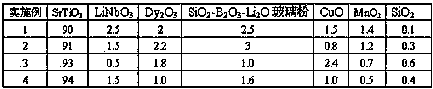
[0020] The present invention will be further described in conjunction with embodiment now. Table 1 provides the formulas of a total of 4 samples of the embodiment of the present invention.

[0021] The main raw material of the formula of the embodiment of the present invention totally 4 samples adopts ceramic capacitor grade pure raw material, at first adopts conventional chemical raw material to synthesize SrTiO respectively with solid-phase method during preparation 3 , LiNbO 3 , SiO 2 -B 2 o 3 -Li 2 O glass powder, then batching according to the above formula, mix the prepared material with distilled water or deionized water by planetary ball mill ball mill, material: ball: water = 1:3: (0.6~1.0) (mass ratio), ball mill 4~ After 8 hours, dry the dry powder, add 8-10% by weight of polyvinyl alcohol solution with a concentration of 10% to the dry powder, granulate, pass through a 40-mesh sieve after mixing, and then sieve at 20-30Mpa Carry out dry pressing under p...


PUM

PropertyMeasurementUnit
dielectric lossaaaaaaaaaa

Abstract

The invention relates to the technical field of inorganic non-metal materials, and particularly discloses a low temperature coefficient crystal boundary layer ceramic capacitor medium and a preparation method thereof. The medium formula comprises the following components in percentage by weight: 88 to 96 percent of SrTiO3, 0.1 to 4 percent of LiNbO3, 0.05 to 4 percent of Dy2O3, 0.03 to 3.0 percent of SiO2-B2O3-Li2O glass powder, 0.1 to 4 percent of CuO, 0.01 to 1 percent of SiO2, and 0.03 to 2.0 percent of MnO, wherein SrTiO3, LiNbO3 and SiO2-B2O3-Li2O glass powder are respectively compounded by conventional chemical raw materials through a solid phase method. According to the invention, a conventional ceramic capacitor medium preparation method and a one-time sintering technological method are adopted, the common capacitor ceramic chemical raw material is adopted to prepare the lead-free and cadmium-free low temperature coefficient crystal boundary layer ceramic capacitor medium, the sintering temperature of capacitor ceramic can be also lowered, and the medium is applicable to the preparation of monolithic ceramic capacitors and monolayer chip ceramic capacitors.

Description

technical field [0001] The invention relates to the technical field of inorganic non-metallic materials, in particular to a low temperature coefficient grain boundary layer ceramic capacitor medium and a preparation method thereof, which adopts a conventional ceramic capacitor medium preparation method and a one-time sintering process, and utilizes common chemical raw materials of capacitor ceramics, The lead-free and cadmium-free low temperature coefficient grain boundary layer ceramic capacitor medium can be prepared, which can also reduce the sintering temperature of capacitor ceramics. This medium is suitable for preparing monolithic ceramic capacitors and single-layer chip ceramic capacitors, and can greatly reduce the ceramic capacitor Cost, the dielectric constant of the medium is high, it is easy to realize the miniaturization of ceramic capacitors, and at the same time, it can increase the withstand voltage to expand the application range of grain boundary layer cerami...

Claims


Application Information

Patent Timeline
Patent Type & Authority Applications(China)
IPC IPC(8): C04B35/47C04B35/622
Inventor 高春华黄新友李军
Owner JIANGSU UNIV
Why Eureka
Try Eureka