A psoi lateral high voltage power semiconductor device

A power semiconductor, lateral high-voltage technology, applied in semiconductor devices, electrical components, circuits, etc., can solve the problems of low breakdown voltage of high-voltage power devices, inability to introduce heat into the substrate, and poor thermal conductivity of the buried oxide layer, so as to improve the breakdown voltage. voltage, improving self-heating effect, reducing power consumption

Inactive Publication Date: 2015-12-09
UNIV OF ELECTRONICS SCI & TECH OF CHINA
View PDF5 Cites 0 Cited by
  • Summary
  • Abstract
  • Description
  • Claims
  • Application Information

AI Technical Summary

Problems solved by technology

However, SOI currently faces two problems: (1) The buried oxide layer blocks the potential lines from penetrating into the substrate, making the power lines of the top silicon dense, and avalanche breakdown occurs in advance, resulting in a low breakdown voltage of SOI high-voltage power devices; (2) ) The poor thermal conductivity of the buried oxide layer prevents the heat generated in the active area from being introduced into the substrate, resulting in high device temperature and obvious self-heating effect

Method used


Image

  • A psoi lateral high voltage power semiconductor device
  • A psoi lateral high voltage power semiconductor device
  • A psoi lateral high voltage power semiconductor device

Examples


Embodiment

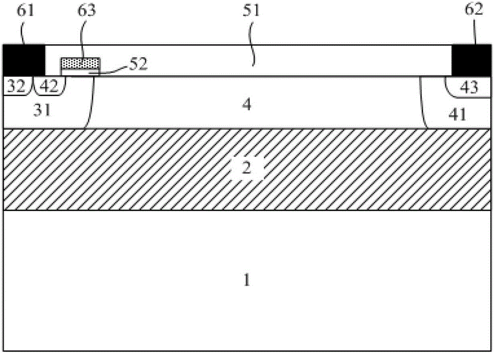
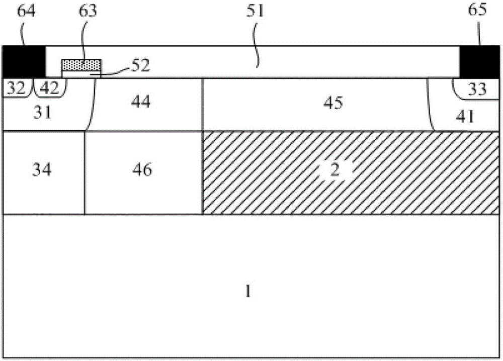
[0036] Such as figure 2As shown, in the PSOI lateral high-voltage power semiconductor device provided in this example, the first conductive type semiconductor buried layer 34 and the second conductive type semiconductor buried layer 46 are introduced into the silicon window to alleviate the self-heating effect of the high-voltage device, wherein, The first conductive type semiconductor buried layer 34 may or may not have it. The introduced semiconductor buried layer 46 of the second conductivity type provides a larger conduction area for carriers when it is in an on state, avoiding excessive concentration of carriers at the source end, thereby reducing device heat loss and alleviating self-heating effects. The drift region of the device is composed of a first drift region 44 of a semiconductor of the second conductivity type and a second drift region 45 of a semiconductor of the second conductivity type, wherein the second drift region 45 of the semiconductor of the second co...


PUM


Abstract

The invention relates to the technology of semiconductors, in particular to a PSOI transverse high-voltage power semiconductor device. The transverse high-voltage MOSFET is characterized in that a second conductive type semiconductor buried layer is introduced below a source end, current carries are prevented from being too concentrated at the source end, power consumption of the device at the source end is reduced, and therefore natural heat effect of the device is improved; even doping is adopted in a first drift region of a second conductive type semiconductor, doping relatively high in concentration is adopted in a second drift region of the second conductive type semiconductor, electrical resistivity of the drift regions can be reduced, specific on-resistance of the device is reduced, and therefore power consumption of the device is reduced, and temperature of the device is lowered. The PSOI transverse high-voltage power semiconductor device has the advantages of being good in self-heating effect, low in on-resistance, high in voltage resistance, small in domain area and the like, and technological difficulty and cost are reduced.

Description

technical field [0001] The invention relates to semiconductor technology, in particular to a PSOI (Partial Silicon-On-Insulator) lateral high-voltage power semiconductor device. Background technique [0002] SOI (Silicon-On-Insulator) has the characteristics of ideal dielectric isolation, high integration, small parasitic effects, and strong radiation resistance. It is a promising low-power device, especially suitable for radio frequency amplifiers or micro power integrated circuits. However, SOI currently faces two problems: (1) The buried oxide layer blocks the potential lines from penetrating into the substrate, making the power lines of the top silicon dense, and avalanche breakdown occurs in advance, resulting in a low breakdown voltage of SOI high-voltage power devices; (2) ) The poor thermal conductivity of the buried oxide layer prevents the heat generated in the active region from being introduced into the substrate, resulting in high device temperature and obvious...

Claims


Application Information

Patent Timeline
Patent Type & Authority Patents(China)
IPC IPC(8): H01L29/739H01L29/06
CPCH01L29/0603H01L29/7393
Inventor 乔明李燕妃许琬胡利志吴文杰蔡林希陈涛张波
Owner UNIV OF ELECTRONICS SCI & TECH OF CHINA
Why Eureka
Try Eureka