A Broadband Printed Dipole Antenna with Novel Branch Line Integrated Feed Balun
A technology of dipole antenna and feed balun, which is applied in the direction of feed, slot antenna, resonant antenna, etc. in the middle position between the antenna ends, which can solve the unfavorable miniaturization and simplification of antenna design, and the inapplicability of printed dipoles Sub-antenna design, unfavorable cross-structure array design, etc., to overcome the narrow bandwidth of printed dipoles, facilitate integrated design, and increase processing complexity
- Summary
- Abstract
- Description
- Claims
- Application Information
AI Technical Summary
Problems solved by technology
Method used
Image
Examples
Embodiment 1
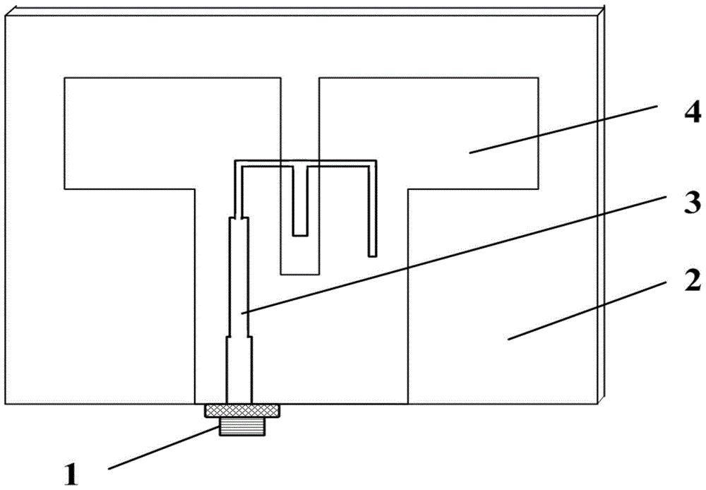
[0039] Embodiment 1, single layer structure antenna
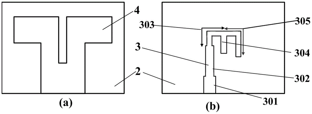
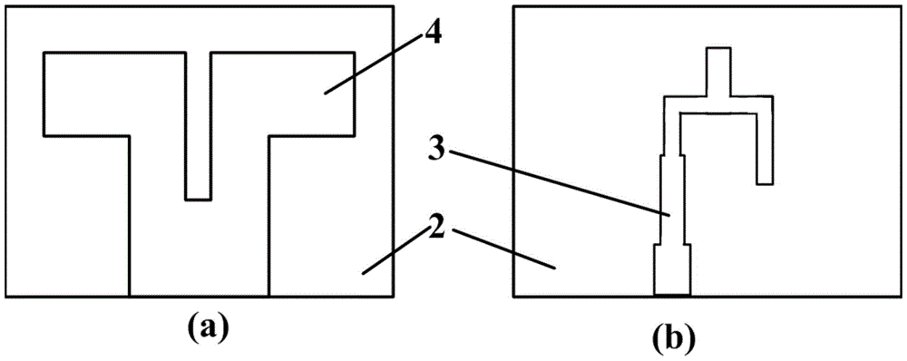
[0040] The dielectric board 2 is an FR4 dielectric board with a dielectric constant of 4.4 and a thickness of 1.5 mm, with a length of 82 mm and a width of 62 mm. The length of the upper end of the radiation unit 4 is 72 mm, about half the wavelength of the center frequency of 2.3 GHz, and the width is 23 mm. The height of the radiation unit 4 is 55 mm, and the width of the lower end is 30 mm. In the middle of the radiation unit 4, there is a slot with a width of 5 mm and a length of 32 mm.
[0041] The total height of the microstrip feed integrated balun 3 on the opposite side of the dielectric board 2 is 39.8 mm. The microstrip line 301 with a characteristic impedance of 50 ohms has a length of 11 mm and a width of 2.8 mm. The first-stage impedance transformation section 302 is 20 mm long and 2 mm wide. The width of the second fold line impedance transformation section 303 is 0.8mm, the length of the vertical section i...
Embodiment 2
[0045] Embodiment 2, double-layer structure plus reflector antenna
[0046] refer to Figure 4 , according to the antenna with the single-layer structure above, a double-layer dielectric board structure antenna is designed. Such as Figure 4 , further includes a metal reflector 5, the dielectric plate 2 is two pieces, the two dielectric plates 2 are stacked together to form a double-layer dielectric plate, the double-layer dielectric plate is vertically arranged on the metal reflector 5, the double-layer dielectric The aforementioned radiation unit 4 is printed on both outer surfaces of the board, and the aforementioned stripline integrated feed balun 3 is printed on the middle interlayer of the double-layer dielectric board.
[0047] Dielectric plate 2 selects the FR4 medium plate that dielectric constant is 4.4, thickness is 1.5mm for use, and the metal reflector 5 top that adds is long 92mm, and height is 64mm, medium plate; Metal reflector 5 lower end dielectric plates a...
PUM
 Abstract
Description
Claims
Application Information


