Semi-conductor laser device capable of outputting double-wavelength laser for optical mixing to generate THz waves and manufacturing method

A manufacturing method and a technology for outputting light, which are applied to the structure of optical waveguide semiconductors and the structure of active regions, etc., can solve the problems of increased volume, long assembly time, and increased cost, and achieve increased volume, long assembly time, and Effect of cost increase

Inactive Publication Date: 2014-02-05
BEIJING UNIV OF TECH
View PDF2 Cites 12 Cited by
  • Summary
  • Abstract
  • Description
  • Claims
  • Application Information

AI Technical Summary

Problems solved by technology

Using two independent semiconductor lasers to achieve photon mixing can obtain continuous THz radiation, but combining discrete las...

Method used


Image

  • Semi-conductor laser device capable of outputting double-wavelength laser for optical mixing to generate THz waves and manufacturing method

Examples


Embodiment Construction

[0025] The present invention will be further described below in conjunction with the accompanying drawings.

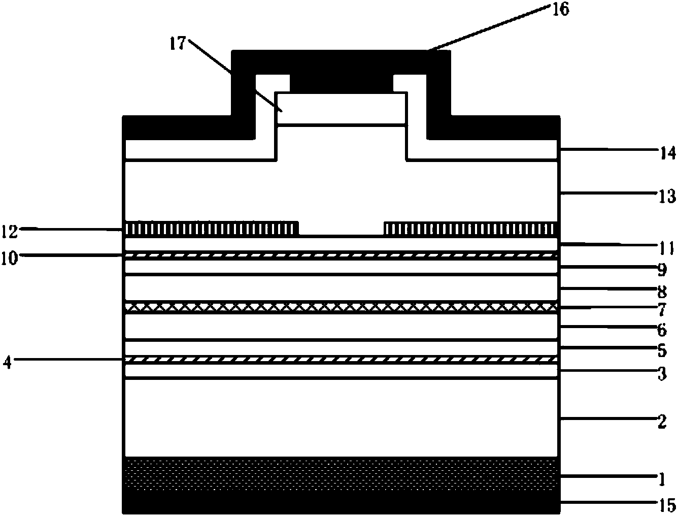
[0026] As shown in the accompanying drawing, it is a schematic lateral cross-sectional view of a semiconductor laser with dual-wavelength output light mixed to generate terahertz waves provided by the present invention, including: substrate 1, N-type confinement layer 2, lower waveguide layer I3, and active layer I4 , Upper waveguide layer I5, P-type confinement layer 6, regeneration mechanism 7, N-type confinement layer 8, lower waveguide layer II9, active layer II10, upper waveguide layer II11, current blocking layer 12, P-type confinement layer 13, dioxide Silicon insulating layer 14 , lower N-type electrode 15 , upper P-type electrode 16 , and P-type ohmic contact layer 17 .

[0027] The specific preparation method of the present invention has the following steps:

[0028] Step 1, growing lower confinement layer I2, active layer I4, upper confinement layer I6, reg...


PUM


Abstract

The invention relates to a semi-conductor laser device capable of outputting double-wavelength laser for optical mixing to generate THz waves and a manufacturing method. The semi-conductor laser device comprises a semi-conductor laser device epitaxy structure formed by a substrate, a lower limiting layer I, a lower waveguide layer I, an active layer I, an upper waveguide layer I, an upper limiting layer I, a regenerating mechanism, a lower limiting layer II, a lower waveguide layer II, an active layer II, an upper waveguide layer II, current blocking layers, an upper limiting layer II and a P-type Ohm contact layer. The two current blocking layers are formed on the two sides of the longitudinal shaft of the semi-conductor laser device respectively in a wet oxidation method or a proton bombard method, and the current spreading effect of the active area II is effectively prohibited. The THz waves generated by optical mixing achieved through the double-length laser are easy to produce and achieve, light output through optical cavity coupling is coaxial, and synchronous control is achieved. The coaxial double-wavelength semi-conductor laser device enables a THz source to be simple in structure, cost is reduced, continuous output power is large, and the THz source can work at the room temperature.

Description

technical field [0001] The invention relates to a semiconductor laser and a manufacturing method, belonging to the technical field of semiconductor optoelectronics, in particular to a semiconductor laser and a manufacturing method for dual-wavelength output light mixing to generate terahertz waves. Background technique [0002] Terahertz (THz, 1THz=1012Hz) usually refers to a fairly wide range of electromagnetic radiation between millimeter waves and infrared light with a frequency from 0.1THz to 10THz, and is in the transition stage from macroelectronics to microphotonics. Terahertz rays exist widely in nature. For example, the thermal radiation of most surrounding objects has terahertz radiation, and most of the cosmic background radiation spectrum is in the terahertz frequency band. In recent years, due to the broad application prospects of the special band of THz waves in environmental monitoring, biological and medical engineering, astronomy, material science engineerin...

Claims


Application Information

Patent Timeline
IPC IPC(8): H01S5/30H01S5/20H01S5/22
Inventor 崔碧峰凌小涵张松王晓玲
Owner BEIJING UNIV OF TECH
Why Eureka
Try Eureka