Inverted bottom-emitting organic electroluminescence device and manufacturing method thereof

An electroluminescence and bottom emission technology, applied in the field of inverted bottom emission organic electroluminescence devices and their preparation, can solve the problems of inconsistent evaporation temperature, reduced exciton recombination probability, difficult evaporation temperature, etc. Light scattering, the effect of increasing the transmission rate

Inactive Publication Date: 2014-02-12
OCEANS KING LIGHTING SCI&TECH CO LTD +1
View PDF0 Cites 4 Cited by
  • Summary
  • Abstract
  • Description
  • Claims
  • Application Information

AI Technical Summary

Problems solved by technology

[0004] In traditional light-emitting devices, an electron transport layer is generally prepared to increase the electron transport rate, and an electron injection layer is prepared to improve the electron injection efficiency, and the electron transport rate is usually lower than the hole transport rate. Two or three orders of magnitude. Therefore, the electron transport layer is usually n-doped, that is, the electron transport layer is doped with metal, such as doping Cs salt into Bphen and Li salt into TPBi to improve Electron transfer rate, this method is widely used, and can effectively increase the electron transfer rate, but the evaporation temperature is inconsistent between organic matter and inorganic matter, which brings difficulties to the evaporation temperature, and the rate increase is not high. In addition, the thickness cannot If it is made too thin (below 40nm), when the luminescent material is close to the metal electrode, the luminescent material will couple with the metal electrode, causing a loss to the excitons (surface plasmon waves), and the thickness is too thick (higher than 100nm), the number of defects increases, and the existence of electron traps will cause electrons or holes to enter the traps, resulting in a decrease in the probability of exciton recombination; all of these will affect the increase in electron transmission rate, which will lead to low luminous efficiency

Method used


Image

  • Inverted bottom-emitting organic electroluminescence device and manufacturing method thereof
  • Inverted bottom-emitting organic electroluminescence device and manufacturing method thereof

Examples


Embodiment 1

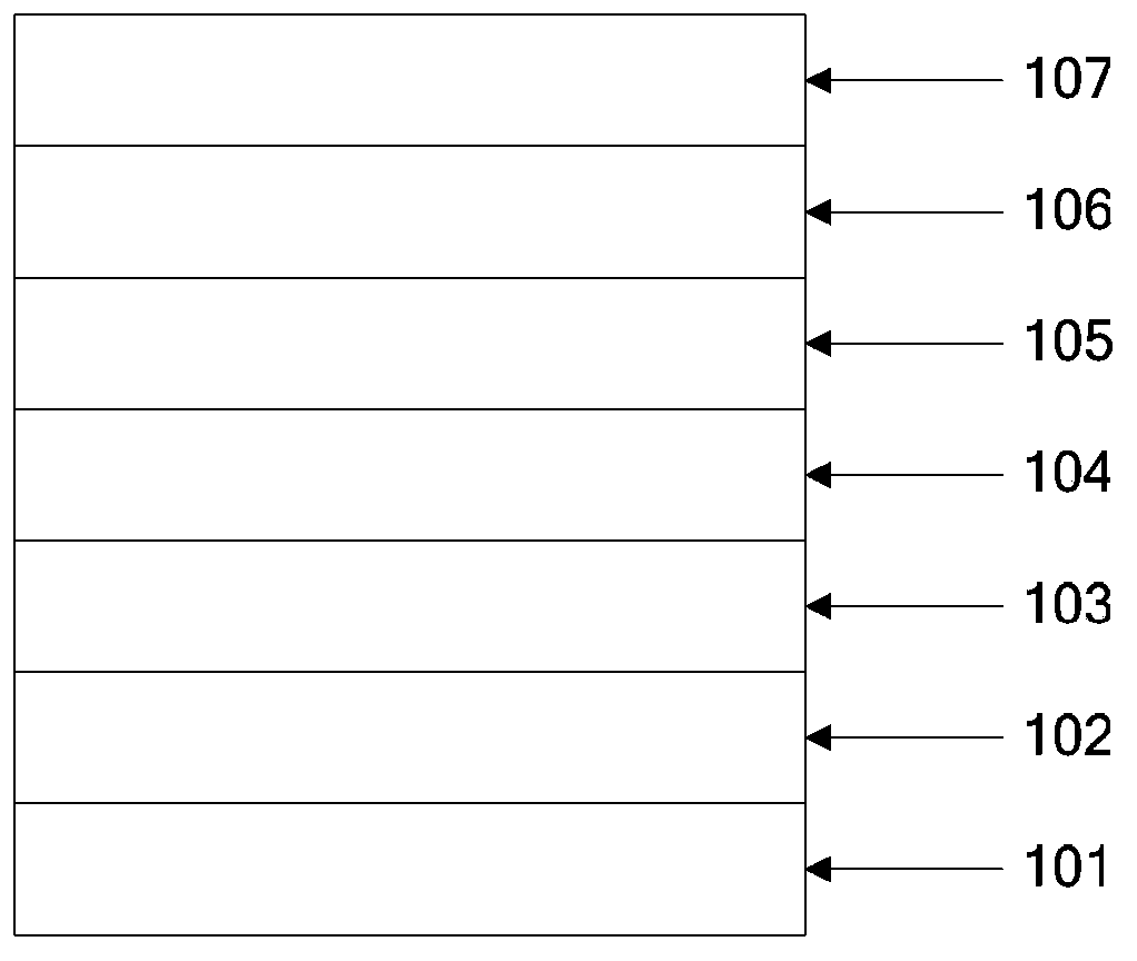
[0040] First, the ITO glass is subjected to photolithography treatment, cut into the required size, and the organic pollutants on the surface of the ITO glass are removed with detergent, deionized water, acetone, ethanol, and isopropanol for 15 minutes each;

[0041] Then spin-coat the auxiliary electron transport layer: first, P3HT is doped into TPBi according to the ratio of 2% by mass to form a doped mixed material, which is expressed as P3HT:TPBi; secondly, the doped mixed material is dissolved in chlorobenzene In , configure a polythiophene solution with a mass percent concentration of 5%; then, spin-coat the polythiophene solution on the surface of the ITO layer of ITO glass, and control the thickness of the spin coating to 100 nm; finally, at 100 ° C annealing to prepare an auxiliary electron transport layer;

[0042] Next, on the surface of the auxiliary electron transport layer, the first electron transport layer is sequentially laminated and evaporated, the material ...

Embodiment 2

[0045] First, the IZO glass is photolithographically processed, cut into the required size, and then ultrasonicated for 15 minutes with detergent, deionized water, acetone, ethanol, and isopropanol to remove organic pollutants on the surface of the IZO glass;

[0046] Then spin-coat the auxiliary electron transport layer: first, P3AT is doped into TPBi according to the ratio of 1% by mass to form a doped mixed material, which is expressed as P3AT:Bphen; secondly, the doped mixed material is dissolved in toluene , configured as a polythiophene solution with a mass percent concentration of 20%; then, spin-coat the polythiophene solution on the surface of the IZO layer of IZO glass, and control the thickness of the spin coating to 200nm; finally, anneal at 100°C processing to obtain an auxiliary electron transport layer;

[0047] Next, on the surface of the auxiliary electron transport layer, the first electron transport layer is sequentially laminated and evaporated, the materia...

Embodiment 3

[0050] First, the IZO glass is photolithographically processed, cut into the required size, and then ultrasonicated for 15 minutes with detergent, deionized water, acetone, ethanol, and isopropanol to remove organic pollutants on the surface of the IZO glass;

[0051] Then spin-coat the auxiliary electron transport layer: first, poly-12-alkylthiophene is doped into TAZ according to the ratio of 5% by mass to form a doped mixed material, which is expressed as poly-12-alkylthiophene: TAZ; secondly, The doped mixed material is dissolved in dichlorobenzene, configured as a polythiophene solution with a mass percent concentration of 10%; then, the polythiophene solution is spin-coated on the surface of the IZO layer of IZO glass, and the spin coating is controlled to The thickness is 10nm; finally, it is annealed at 100°C to obtain an auxiliary electron transport layer;

[0052] Next, on the surface of the auxiliary electron transport layer, the first electron transport layer is se...


PUM

PropertyMeasurementUnit
thicknessaaaaaaaaaa
thicknessaaaaaaaaaa
thicknessaaaaaaaaaa

Abstract

The invention belongs to the field of electroluminescence devices and discloses an inverted bottom-emitting organic electroluminescence device and a manufacturing method thereof. The device comprises a cathode substrate, an auxiliary electronic transmission layer, a first electronic transmission layer, a light-emitting layer, a hole transporting layer, a hole injection layer and an anode layer which are sequentially stacked. The auxiliary electronic transmission layer is made from a doped mixed material formed by doping 1-5% by mass of thiophene polymer into 4,7-diphenyl-1,10-phenanthroline, 1,2,4-triazole derivative or N-aryl benzimidazole. The inverted bottom-emitting organic electroluminescence device can avoid an excitor and metal electrode surface plasmon polariton wave phenomenon, meanwhile enhance light scattering and the front-side luminous intensity and greatly improve the luminous efficiency.

Description

technical field [0001] The invention relates to a light-emitting device, in particular to an inverted bottom-emitting organic electroluminescence device and a preparation method thereof. Background technique [0002] In 1987, C.W.Tang and Van Slyke of Eastman Kodak Company in the United States reported a breakthrough in the research of organic electroluminescence. A high-brightness, high-efficiency double-layer organic electroluminescent device (OLED) has been prepared using ultra-thin film technology. In this double-layer structure device, the brightness reaches 1000cd / m at 10V 2 , its luminous efficiency is 1.51lm / W, and its lifespan is more than 100 hours. [0003] The principle of OLED light emission is based on the action of an external electric field, electrons are injected from the cathode to the lowest unoccupied molecular orbital (LUMO) of organic matter, and holes are injected from the anode to the highest occupied orbital (HOMO) of organic matter. Electrons and...

Claims


Application Information

Patent Timeline
Patent Type & Authority Applications(China)
IPC IPC(8): H01L51/52H01L51/54H01L51/56C09K11/06
CPCH10K85/111H10K50/166H10K50/165H10K50/854H10K2102/321H10K71/00
Inventor 周明杰王平黄辉陈吉星
Owner OCEANS KING LIGHTING SCI&TECH CO LTD
Why Eureka
Try Eureka