Organic solar cell with metal-mesh-nested heterogeneous junctions and preparation method for organic solar cell
A solar cell and metal mesh technology, applied in circuits, photovoltaic power generation, electrical components, etc., can solve the problems of weak built-in electric field and low conversion efficiency of organic solar cells, achieve strong electron affinity, increase built-in electric field strength, increase Effect of Structure Thickness
- Summary
- Abstract
- Description
- Claims
- Application Information
AI Technical Summary
Problems solved by technology
Method used
Image
Examples
Embodiment 1
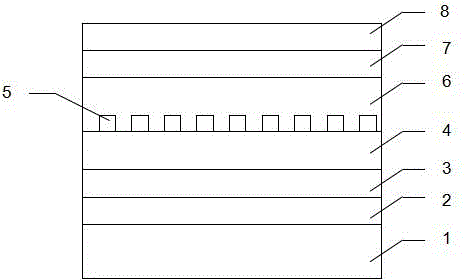
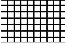
[0043] Device structure such as figure 1 shown. The material and thickness of each layer of the device are: substrate 1 is glass, anode electrode 2 is ITO with a thickness of 180 nm, hole transport layer 3 is copper phthalocyanine CuPc and perfluorophthalocyanine copper F 16 A mixed layer of CuPc with a thickness of 10 nm and a donor material of poly-3-hexylthiophene P 3 HT, the thickness is 30nm, the ultra-thin mesh metal layer is Ag, the thickness of the mesh metal layer is 1nm, the acceptor material is fullerene derivative PC61BM, the thickness is 40nm, the electron buffer layer is 4,7-diphenyl O-phenanthroline Bphen, the thickness is 2.5nm, the cathode is Ag, the thickness is 150nm.
[0044] Its preparation method is as follows:
[0045] ①Use detergent, acetone solution, deionized water and ethanol solution to ultrasonically clean the glass substrate on which the transparent anode electrode ITO has been sputtered, and dry it with dry nitrogen after cleaning;
[0046] ②...
Embodiment 2
[0054] Device structure such as figure 1 shown. The material and thickness of each layer of the device are as follows: the substrate 1 is glass, the anode electrode 2 is ITO with a thickness of 180 nm, and the hole transport layer 3 is copper phthalocyanine CuPc and perfluorophthalocyanine copper F 16 A mixed layer of CuPc with a thickness of 10 nm and a donor material of poly[[9-(1-octylnonyl)-9H-carbazole-2,7-diyl]-2,5-thiophenediyl-2,1 ,3-benzothiadiazole-4,7-diyl-2,5-thiophenediyl] (PCDTBT), the thickness is 30nm, the ultra-thin mesh metal layer is Au, the thickness of the metal layer is 1nm, the acceptor The material is fullerene derivative PC71BM with a thickness of 40nm, the electron buffer layer is 4,7-diphenyl-phenanthroline (Bphen) with a thickness of 2.5nm, and the cathode is Ag with a thickness of 150nm. The preparation process is similar to Example 1.
experiment example 3
[0056] Device structure such as figure 1 shown. The material and thickness of each layer of the device are: substrate 1 is glass, anode electrode 2 is ITO with a thickness of 180 nm, and hole transport layer 3 is 5,5'-bis(4-biphenyl)-2,2' - A mixed layer of dithiophene (BP2T) and perfluorophthalocyanine copper (F16CuPc) with a thickness of 10 nm, a donor material of poly-3-hexylthiophene (P3HT) with a thickness of 30 nm, and an ultra-thin metal layer of Pt with a thickness of 1nm, the acceptor material is fullerene derivative PC61BM, the thickness is 40nm, the electron buffer layer is 4,7-diphenyl-phenanthroline (Bphen), the thickness is 2.5nm, the cathode is Ag, the thickness is 150nm. The preparation process is similar to Example 1.
PUM
 Abstract
Description
Claims
Application Information


