Preparation method for transparent conductive metal network

A metal network, transparent and conductive technology, applied in metal material coating process, ion implantation plating, coating, etc., can solve problems such as insoluble resin, damage, nanowire substrate detachment, etc., to achieve online production and avoid engraving The effect of eclipse, active connection

Active Publication Date: 2014-03-12
苏州冷石纳米材料科技有限公司
View PDF5 Cites 15 Cited by
  • Summary
  • Abstract
  • Description
  • Claims
  • Application Information

AI Technical Summary

Problems solved by technology

[0004] At present, there have been many patent applications for transparent conductive films based on silver nanowires, but the usual processing technology is relatively complicated, and it takes several steps of transfer printing or repeated coating processes to finally achieve the required results.
Chinese patent applications 200910112924.X and 200910112925.4 disclose a method for preparing a transparent conductive film based on silver nanowires. The core idea is to increase the adhesion of silver nanowires on the substrate by adding an adhesion layer between the substrate and the nanowire conductive layer. Efforts have been made to basically solve the problem that the nanowires are easy to detach from the substrate, but the method used is relatively complicated, and the pre-prepared nanowire network needs to be transferred to the adhesion layer by transfer printing, which not only increases the difficulty of the process and Complexity, while the thickness of the silver nanowire network is difficult to control, which affects the light transmission of the final conductive film
The layering preparation process is complicated, and each layer needs to be dried after coating, which takes a long time and processing a new layer will inevitably cause damage to the existing layer, and the product yield will be greatly affected
Chinese patent application 201110444509.1 discloses another preparation method of transparent conductive film based on silver nanowires, which realizes a wide range of haze adjustment, but the polymer binders used in this patent are all insoluble resins, and the film formation is dry. Sometimes it will cause uneven crystallization and affect the light transmittance of the final film. At the same time, this method can only obtain an overall conductive initial film, which cannot meet the requirements of the touch terminal for electrode pattern design.

Method used


Image

  • Preparation method for transparent conductive metal network
  • Preparation method for transparent conductive metal network
  • Preparation method for transparent conductive metal network

Examples


Embodiment 1

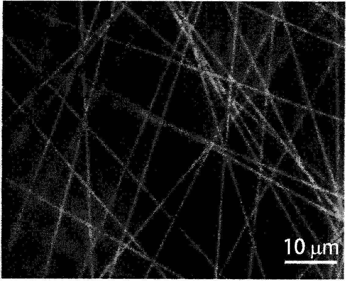
[0031] Preparation of polyvinyl alcohol nanofiber network:

[0032] First, take 2 grams of polyvinyl alcohol in 20 grams of water, heat and stir to dissolve until uniform, transfer it to a 30 ml syringe after it is completely dissolved, place it under 15kV high voltage, perform electrospinning, and arrange it in an orderly manner according to the required pattern A polyvinyl alcohol nanofiber network with a diameter of about 200 nm and a length of about 2 cm was obtained; the obtained polymer fiber network was then baked at 80° C. for 20 minutes to obtain a dried fiber network.

[0033] Preparation of metal conductive network:

[0034]The obtained dried polyvinyl alcohol nanofiber network is placed in a magnetron sputtering furnace, and a silver layer with a thickness of 40 nanometers is sputtered on the surface of the polyvinyl alcohol nanofiber network at a temperature of 60 ° C to obtain a silver-polyvinyl alcohol nanofiber network. fiber composite network. Then put this ...

Embodiment 2

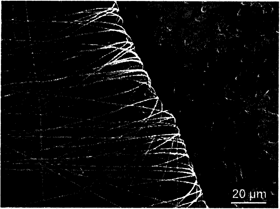
[0040] Firstly, take 2.4 grams of polyvinylpyrrolidone, heat and stir it in 20 grams of water to dissolve until uniform, transfer it to a 30 ml syringe after it is completely dissolved, place it under 15kV high voltage, conduct electrospinning, and arrange it in an orderly manner according to the required pattern A polyvinylpyrrolidone nanofiber network with a diameter of about 150 nm and a length of about 3 cm was obtained; the obtained polymer fiber network was then baked at 60° C. for 30 minutes to obtain a dried fiber network.

[0041] Preparation of metal conductive network:

[0042] The obtained dried polyvinylpyrrolidone nanofiber network is placed in a magnetron sputtering furnace, and a gold layer with a thickness of 20 nanometers is sputtered on the surface of the polyvinylpyrrolidone nanofiber network at a temperature of 60 ° C to obtain gold-polyvinylpyrrolidone nanofiber network. fiber composite network. Then put this composite network structure in an ethanol sol...

Embodiment 3

[0046] First, take 1.5 grams of hydroxypropyl methylcellulose in 20 grams of water, heat and stir to dissolve until uniform, transfer it to a 30 ml syringe after it is completely dissolved, place it under a high voltage of 15kV, and carry out electrospinning, and carry out organic spinning according to the required pattern. A hydroxypropyl methylcellulose nanofiber network with a diameter of about 250 nanometers and a length of about 5 cm can be obtained by sequential arrangement; then the obtained polymer fiber network is baked at 60°C for 30 minutes to obtain a dried fiber network .

[0047] Preparation of metal conductive network:

[0048] The obtained dried hydroxypropyl methylcellulose nanofiber network is placed in a magnetron sputtering furnace, and a copper coating with a thickness of 50 nanometers is sputtered on the surface of the polyvinylpyrrolidone nanofiber network at a temperature of 60 ° C to obtain copper- Hydroxypropyl methylcellulose nanofiber composite net...


PUM

PropertyMeasurementUnit
lengthaaaaaaaaaa
thicknessaaaaaaaaaa
diameteraaaaaaaaaa

Abstract

The invention discloses a preparation method for a transparent conductive metal network. The preparation method comprises the following steps: a) preparing a nanofiber network through electrospinning; b) evaporating a metal layer on the nanofiber network so as to obtain a metal-polymer network complex; and c) removing a metal in the metal-polymer network complex so as to obtain the transparent conductive metal network. The invention has the following beneficial effects: downstream tedious etching and patterning processes are avoided in preparation of a conductive film prepared from the flexible transparent metal network, demands of touch screens and display panels for patterning can be directly met, and online production can be realized.

Description

technical field [0001] The invention relates to a preparation method of a transparent conductive metal network. Background technique [0002] As a functional film with high light transmittance and low sheet resistance, transparent conductive film is widely used in touch screens, display panels, electromagnetic shielding, LED displays, electroluminescent devices, and thin-film solar cells. Especially in recent years, with the rapid development of touch products, there is a huge demand for transparent conductive films, and at the same time, many problems of traditional transparent conductive films based on indium tin oxide (ITO) have been exposed. Although the traditional ITO transparent conductive film can achieve a film resistance value of less than 10Ω / □ under the premise of 80% visible light transmittance, the resistivity is lower than 1.5×10-42·cm-1. The main problems of ITO transparent conductive films are as follows: (1) The key element indium in ITO faces a relatively...

Claims


Application Information

Patent Timeline
Patent Type & Authority Applications(China)
IPC IPC(8): C23C14/20C23C14/35C23C14/58C22C1/08D01D5/00
Inventor 谷小虎丁轶黄友科王正元
Owner 苏州冷石纳米材料科技有限公司
Why Eureka
Try Eureka