TSV (through silicon via) high-frequency three-dimensional integrated interconnection structure based on SOI (silicon on insulator)

An interconnect structure and three-dimensional technology, applied in the field of microelectronics, can solve the problems of reducing device reliability, reducing economic efficiency, and serious leakage loss, etc., and achieve the effects of reducing noise coupling crosstalk, improving transmission quality, and reducing leakage loss

Active Publication Date: 2014-03-12
珠海天成先进半导体科技有限公司
View PDF6 Cites 8 Cited by
  • Summary
  • Abstract
  • Description
  • Claims
  • Application Information

AI Technical Summary

Problems solved by technology

During high-frequency signal transmission, since silicon has certain conductivity, this sandwich structure exhibits obvious capacitive charging and discharging characteristics, resulting in a part of the signal being lost in silicon through the insulating layer.
As the signal frequency increases, the leakage loss will become more and more serious, and the signal amplitude will be greatly reduced, which will seriously affect the performance of the three-dimensional integrated device
When there are multiple sets of S-G double TSV via interconnect structures (see figure 2 ), the TSV vias used for signal transmission are prone to noise coupling and crosstalk, and signal distortion may cause the three-dimensional integrated device to fail to work normally and reduce the reliability of the device
In addition, due to the need to arrange additional TSV vias for signal return, it will occupy more chip area, which undoubtedly increases development costs and reduces economic efficiency.

Method used


Image

  • TSV (through silicon via) high-frequency three-dimensional integrated interconnection structure based on SOI (silicon on insulator)
  • TSV (through silicon via) high-frequency three-dimensional integrated interconnection structure based on SOI (silicon on insulator)
  • TSV (through silicon via) high-frequency three-dimensional integrated interconnection structure based on SOI (silicon on insulator)

Examples


Embodiment 1

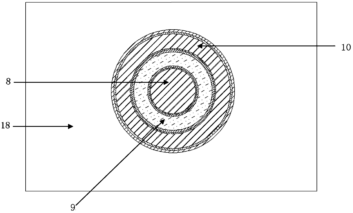
[0017] Such as image 3 As shown, the TSV three-dimensional integrated interconnection structure is based on the SOI substrate 18, the substrate type is P-type silicon, the internal TSV through hole is cylindrical, the external TSV through hole is circular, and the filling between the two is BCB (benzo ring butene resin) fill layer 9.

[0018] Such as Figure 4 As shown, the thickness of the top layer silicon 11 of the SOI substrate 18 is The thickness of the buried oxide layer 12 is The underlying silicon 13 has a thickness of 80 μm. The diameter W1 of the inner cylindrical TSV copper pillar 8 is 15 μm, the thickness D1 of the inner cylindrical TSV through-hole insulation layer 16 is 0.5 μm, the thickness of the inner cylindrical TSV through-hole barrier layer TaN and copper seed layer 17 is 0.4 μm, and the thickness of the TaN layer is D2 is 0.2 μm, and the thickness D3 of the copper seed layer is 0.2 μm. The thickness W2 of the outer annular TSV copper pillar 10 is 6...

Embodiment 2

[0021] Such as image 3 As shown, the TSV three-dimensional integrated interconnection structure is based on the SOI substrate 18, the substrate type is N-type silicon, the internal TSV via hole is cylindrical, the external TSV via hole is annular, and the filling between the two is BCB (benzo ring butene resin) fill layer 9.

[0022] Such as Figure 4 As shown, the thickness of the top layer silicon 11 of the SOI substrate 18 is The thickness of the buried oxide layer 12 is The underlying silicon 13 has a thickness of 100 μm. The diameter W1 of the inner cylindrical TSV copper pillar 8 is 20 μm, the thickness D1 of the inner cylindrical TSV through-hole insulation layer 16 is 0.5 μm, the thickness of the inner cylindrical TSV through-hole barrier layer TaN and copper seed layer 17 is 0.4 μm, and the thickness of the TaN layer is D2 is 0.2 μm, and the thickness D3 of the copper seed layer is 0.2 μm. The thickness W2 of the outer annular TSV copper pillar 10 is 7 μm, the...


PUM

PropertyMeasurementUnit
thicknessaaaaaaaaaa
thicknessaaaaaaaaaa

Abstract

The invention provides a TSV (through silicon via) high-frequency three-dimensional integrated interconnection structure based on SOI (silicon on insulator). An internal cylindrical TSV through hole is coaxial with an external annular TSV through hole, in addition, benzocyclobutene resin insulation glue is filled between the internal cylindrical TSV through hole and the external annular TSV through hole, the external annular STV through hole sequentially comprises a silicon dioxide insulation layer, a blocking layer TaN, a copper seed layer and a hollow copper post from outside to inside, the internal cylindrical TSV through hole also sequentially comprises a silicon dioxide insulation layer, a blocking layer TaN, a copper seed layer and a cylindrical copper post from outside to inside, the silicon dioxide insulation layers, the blocking layers TaN, the seed layers, the hollow copper post and the copper post all penetrate through top layer silicon, a silicon dioxide buried oxide layer and bottom layer silicon of an SOI substrate in the longitudinal direction. The TSV high-frequency three-dimensional integrated interconnection structure has the advantages that the area of a chip is greatly reduced, in addition, signals are mutually insulated and isolated, the electricity leakage consumption and the noise coupling crosstalk are reduced, the signal transmission quality is improved, the reliability of three-dimensional integrated devices is enhanced, and the application requirements of radiation-proof reinforcement of high-frequency three-dimensional integrated devices can be met.

Description

technical field [0001] The invention relates to the technical field of microelectronics. Background technique [0002] In order to meet the application requirements of high-frequency signal transmission of TSV three-dimensional integrated devices, it is usually necessary to design a TSV through-hole interconnection structure with a signal return path. At present, the S-G (signal-ground) double TSV through-hole interconnection structure proposed in the document "High-Frequency Scalable Electrical Model and Analysis of a Through Silicon Via (TSV)" is widely used in TSV three-dimensional integrated devices (see figure 1 ) to transmit high-frequency signals. This interconnection structure consists of two TSV vias, one is used for signal transmission, and the other is used as a "ground" for signal return. The two TSV vias are each wrapped by a silicon dioxide insulating layer and silicon to form a copper / Ta / TaN-Silica-Silicon sandwich structure. During high-frequency signal t...

Claims


Application Information

Patent Timeline
Patent Type & Authority Applications(China)
IPC IPC(8): H01L23/48
Inventor 刘松单光宝谢成民
Owner 珠海天成先进半导体科技有限公司
Why Eureka
Try Eureka