A silicon oxynitride etching method with gentle and smooth sidewall morphology

A technology of silicon oxynitride and silicon oxynitride materials, applied in electrical components, semiconductor/solid-state device manufacturing, circuits, etc., can solve the problems of narrow process window, affect device performance, increase reverse current, etc., to achieve a wide process window, The effect of solving process defects

Active Publication Date: 2016-08-17
STATE GRID CORP OF CHINA +1
View PDF5 Cites 0 Cited by
  • Summary
  • Abstract
  • Description
  • Claims
  • Application Information

AI Technical Summary

Problems solved by technology

Among them, the steps obtained by the wet method are generally gentle, but the characteristic line width is indeed thinned or widened due to lateral undercutting, which increases the difficulty or uncertainty for the design or processing of the device.
In silicon oxynitride high voltage devices, the change of the characteristic line width will greatly affect the performance of the device, such as the decrease of the breakdown voltage and the increase of the reverse current due to the change of the terminal line width.
However, the dry method has a very narrow process window in order to obtain a relatively gentle step, and it is difficult to ensure the stability of the manufacturing process.

Method used


Image

  • A silicon oxynitride etching method with gentle and smooth sidewall morphology
  • A silicon oxynitride etching method with gentle and smooth sidewall morphology
  • A silicon oxynitride etching method with gentle and smooth sidewall morphology

Examples


Embodiment 1

[0028] 1) Cleaning silicon oxide material:

[0029] The 500nm silicon oxide 1 on the silicon to be etched is followed by the following cleaning steps:

[0030] 1# cleaning solution (ammonia: hydrogen peroxide: pure water = 1:1:5), temperature 70° for 5 minutes; 2# cleaning solution (hydrochloric acid: hydrogen peroxide: pure water = 1:1:5), temperature 70° for 5 minutes 5 minutes for ultrasonication with acetone; 5 minutes for ultrasonication with isopropanol; 5 minutes for DI water rinse, dry and set aside.

[0031] 2) Photolithography, the process flow is as follows:

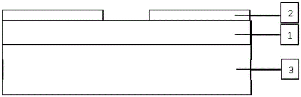
[0032] Vapor-coated tackifier; spin-coated photoresist 3, type 5214, thickness 1.6um; pre-bake at 95 degrees Celsius for 90 seconds; SUSSMA6 lithography machine contact exposure for 7 seconds; develop with 3038 developer for 45s; 110°, 60s to harden the film ,See figure 1 .

[0033] 3) Wet corrosion:

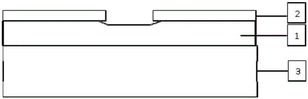
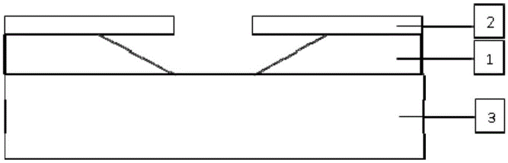
[0034] Wet etching silicon oxide 1 to achieve the purpose of gentle initial steps, the specific process ...

Embodiment 2

[0043] 1) Cleaning silicon nitride material:

[0044] The 500nm silicon nitride material 1 on the silicon to be etched is sequentially subjected to the following cleaning steps:

[0045] 1# cleaning solution (ammonia: hydrogen peroxide: pure water = 1:1:6), temperature 70° for 4 minutes; 2# cleaning solution (hydrochloric acid: hydrogen peroxide: pure water = 1:1:7), temperature 70° for 6 5 points; isopropanol ultrasonication 5 points; acetone ultrasonication 5 points; isopropanol ultrasonication 5 points;

[0046] 2) Photolithography, the process flow is as follows:

[0047] Vapor-coated tackifier; spin-coated photoresist 3, type 5214, thickness 1.6um; pre-bake at 95 degrees Celsius for 90 seconds; SUSSMA6 lithography machine contact exposure for 7 seconds; develop with 3038 developer for 45s; 110°, 60s to harden the film ,See figure 1 .

[0048] 3) Wet corrosion:

[0049] Wet etching silicon nitride material 1 to achieve the purpose of smoothing the initial step, the sp...


PUM


Abstract

The invention relates to a production process of nitrogen, oxygen and silicon devices, in particular to an etching method of nitrogen, oxygen and silicon of gentle and smooth sidewall morphology. The etching method includes rinsing of nitrogen, oxygen and silicon materials, photoetching, wet etching of nitrogen, oxygen and silicon, dry etching of nitrogen, oxygen and silicon, and degumming. The crucial process improvement is that dry etching is combined with wet etching. The etching method changes the traditional process of singly adopting wet etching or dry etching, accordingly solves problems of narrowing of mask strips caused by lateral etching when wet etching is singly adopted and narrow windows when dry etching is singly adopted, and can be used for quickly, effectively and conveniently acquiring the nitrogen, oxygen and silicon etching morphology of gentle and smooth sidewalls.

Description

technical field [0001] The invention relates to a manufacturing process of a silicon oxynitride device, in particular to a silicon oxynitride etching method with gentle and smooth sidewall morphology. Background technique [0002] Semiconductor etching is not only a method of semiconductor surface processing, but also an important patterning method in the semiconductor device manufacturing process. [0003] Silicon oxide or silicon nitride is a commonly used thin film material in semiconductor manufacturing processes. It is often used as insulation passivation, insulation isolation or etching hard mask material. Silicon oxynitride is widely used in in the optical waveguide. In the etching of silicon oxynitride materials, there are mainly two methods: dry method and wet method. The dry method mainly uses F-based gas etching, while the wet method mainly uses HF-based acid solution for etching. The silicon oxynitride etching process with the same gentle step shape generally h...

Claims


Application Information

Patent Timeline
Patent Type & Authority Patents(China)
IPC IPC(8): H01L21/311
CPCH01L21/30604
Inventor 陆敏张昭田亮杨霏
Owner STATE GRID CORP OF CHINA
Why Eureka
Try Eureka