Light-emitting diode epitaxial wafer and manufacture method thereof

A technology for light-emitting diodes and epitaxial wafers, applied in electrical components, circuits, semiconductor devices, etc., can solve the problems of limited improvement of light-emitting diode brightness and low internal quantum efficiency of light-emitting diodes, reducing electron overflow and improving internal quantum efficiency. Efficiency, the effect of increasing the barrier height

Active Publication Date: 2014-03-26
HC SEMITEK SUZHOU
View PDF5 Cites 27 Cited by
  • Summary
  • Abstract
  • Description
  • Claims
  • Application Information

AI Technical Summary

Problems solved by technology

[0005] While blocking electron overflow, the electron blocking layer also blocks the injection of holes into the quantum well, resulting in the low internal quantum efficiency of the light-emitting diode, which in turn leads to a limited increase in the brightness of the light-emitting diode.

Method used


Image

  • Light-emitting diode epitaxial wafer and manufacture method thereof
  • Light-emitting diode epitaxial wafer and manufacture method thereof
  • Light-emitting diode epitaxial wafer and manufacture method thereof

Examples


Embodiment 1

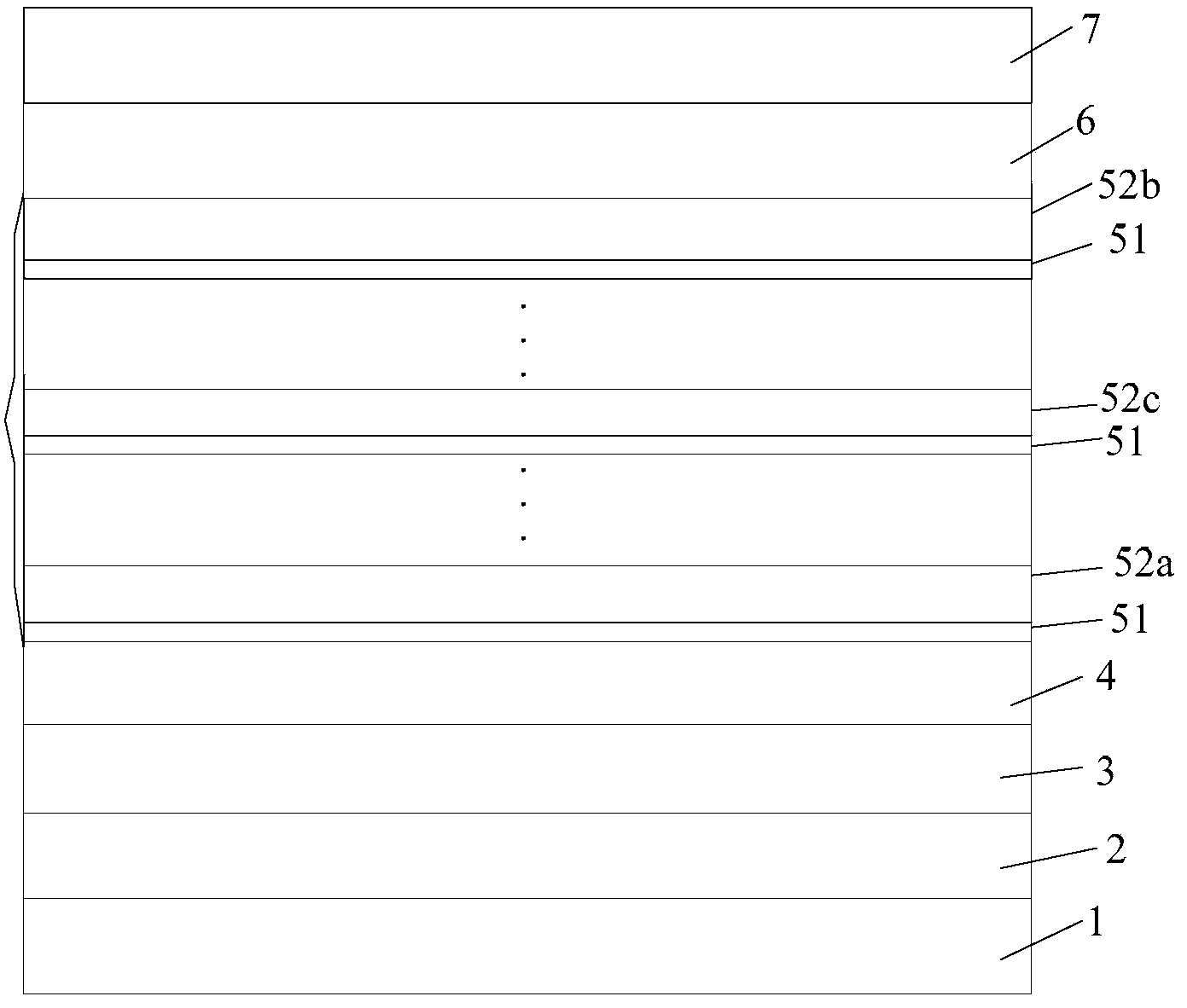
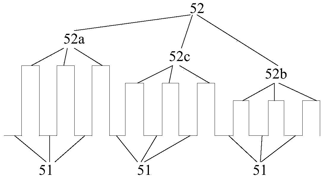
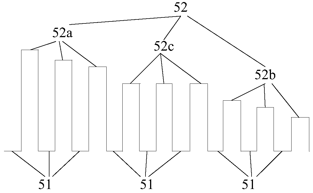
[0030] An embodiment of the present invention provides an epitaxial wafer for a light-emitting diode, see figure 1 , the epitaxial wafer includes a substrate 1, a low temperature buffer layer 2 grown on the substrate 1, an undoped gallium nitride layer 3, an N-type gallium nitride layer 4, a multiple quantum well layer 5 and a P-type gallium nitride layer Layer 6, the multiple quantum well layer 5 is a superlattice structure, the superlattice structure includes a quantum well layer 51 and a quantum barrier layer 52 (see Figure 1a and 1b ), the quantum well layers 51 and the quantum barrier layers 52 are alternately grown, wherein at least one quantum barrier layer 52a starting from the N-type gallium nitride layer side is made of Al x Ga 1-x N growth, 0z Ga 1-z N grows, 0

[0031] Preferably, the period number of the multiple quantum well layer is 5-15, but it is not li...

Embodiment 2

[0050] An embodiment of the present invention provides an epitaxial wafer for a light-emitting diode. The structure of the epitaxial wafer in this embodiment is basically the same as that of the epitaxial wafer in Embodiment 1, except that the multiple quantum well layer 5 of the epitaxial wafer does not include Intermediate quantum barrier layer 52c.

[0051] see figure 2 , the epitaxial wafer includes, from bottom to top, a substrate 1, a low temperature buffer layer 2, an undoped gallium nitride layer 3, an N-type gallium nitride layer 4, a multiple quantum well layer 5 and a P-type gallium nitride layer 6, The multi-quantum well layer 5 is a superlattice structure, and each period includes a quantum well layer 51 and a quantum barrier layer 52, and the quantum well layer 51 and the quantum barrier layer 52 grow alternately, wherein, from the side of the N-type gallium nitride layer. At least one quantum barrier layer 52a uses Al x Ga 1-x N growth, 0z Ga 1-z N grows, 0...

Embodiment 3

[0056] Embodiments of the present invention provide a method for fabricating an epitaxial wafer of a light-emitting diode, see image 3 , methods include:

[0057] Step 301: providing a substrate;

[0058] Optionally, in this embodiment, the substrate includes but is not limited to a sapphire substrate.

[0059] When realized, the substrate can be kept at 1300 °C H 2 The heat treatment was performed in the atmosphere for 10 minutes, and the surface was cleaned.

[0060] Step 302 : growing a low temperature buffer layer, an undoped gallium nitride layer, and an N-type gallium nitride layer on the substrate in sequence;

[0061] Optionally, in this embodiment, the low temperature buffer layer may be a gallium nitride layer, or may be an aluminum nitride layer or an aluminum gallium nitride layer. Specifically, at a temperature of 550° C., a low-temperature buffer layer made of GaN is grown on the surface of the substrate with a thickness of 20-30 nm.

[0062] Specifically, ...


PUM

PropertyMeasurementUnit
thicknessaaaaaaaaaa
thicknessaaaaaaaaaa
thicknessaaaaaaaaaa

Abstract

The invention discloses a light-emitting diode epitaxial wafer and a manufacture method thereof and belongs to the field of semiconductor technology. The epitaxial wafer comprises a substrate, a low-temperature buffer layer grown on the substrate, a non-doped gallium nitride layer, a type-N gallium nitride layer, a multiple-quantum well layer and a type-P gallium nitride layer. At least one quantum barrier from one side of the type-N gallium nitride layer is grown by AlxGa1-xN; 0<x<0.3. At least one quantum barrier layer from one side of the type-P gallium nitride layer is grown by InzGa1-zN; 0<z<0.15. The type-P gallium nitride layer is directly grown on the multiple-quantum well layer. The quantum barrier layers close to the type-N gallium nitride layer are provided with high potential barrier, the quantum barrier layers close to the type-P gallium nitride layer are provided with low potential barrier, electron overflow is reduced, hole injection efficiency is improved, more electrons and holes are composited in the quantum well layer, and internal quantum efficiency of the light-emitting diode is improved accordingly.

Description

technical field [0001] The invention relates to the technical field of semiconductors, in particular to an epitaxial wafer of a light emitting diode and a manufacturing method thereof. Background technique [0002] GaN (gallium nitride) is a typical representative of the third-generation wide-bandgap semiconductor material. Its excellent high thermal conductivity, high temperature resistance, acid and alkali resistance, high hardness and other characteristics make it widely used in the production of blue, green, UV LEDs. A GaN-based light-emitting diode generally includes an epitaxial wafer and electrodes provided on the epitaxial wafer. [0003] An existing GaN-based semiconductor light-emitting epitaxial wafer includes a substrate, and an N-type layer, a multi-quantum well layer, an electron blocking layer and a P-type layer sequentially grown on the substrate, wherein the structure of the multi-quantum well is InGaN / GaN, which confines the carriers, when the forward cur...

Claims


Application Information

Patent Timeline
Patent Type & Authority Applications(China)
IPC IPC(8): H01L33/00H01L33/06
CPCH01L33/0075H01L33/06
Inventor 刘华容魏世祯谢文明
Owner HC SEMITEK SUZHOU
Why Eureka
Try Eureka