High-reliability TSV (Through Silicon Via) technique based on SOI (Silicon-On-Insulator) substrate

A process method and reliability technology, applied in the field of microelectronics, can solve the problems affecting the performance and reliability of SOI three-dimensional integrated devices, difficult metallization of through holes, and increased leakage, so as to achieve high reliability, improve performance, and increase reliability. sexual effect

Active Publication Date: 2014-04-02
珠海天成先进半导体科技有限公司
View PDF6 Cites 18 Cited by
  • Summary
  • Abstract
  • Description
  • Claims
  • Application Information

AI Technical Summary

Problems solved by technology

Due to the existence of the "Notching" structure, it will be difficult to make subsequent insulation layers, barrier layers / seed layers, and through-hole metallization on the side walls of the through-holes. There will be potential safety hazards such as increased leakage and reduced withstand voltage, which will seriously affect the performance and performance of SOI three-dimensional integrated devices. reliability

Method used


Image

  • High-reliability TSV (Through Silicon Via) technique based on SOI (Silicon-On-Insulator) substrate
  • High-reliability TSV (Through Silicon Via) technique based on SOI (Silicon-On-Insulator) substrate
  • High-reliability TSV (Through Silicon Via) technique based on SOI (Silicon-On-Insulator) substrate

Examples


Embodiment 1

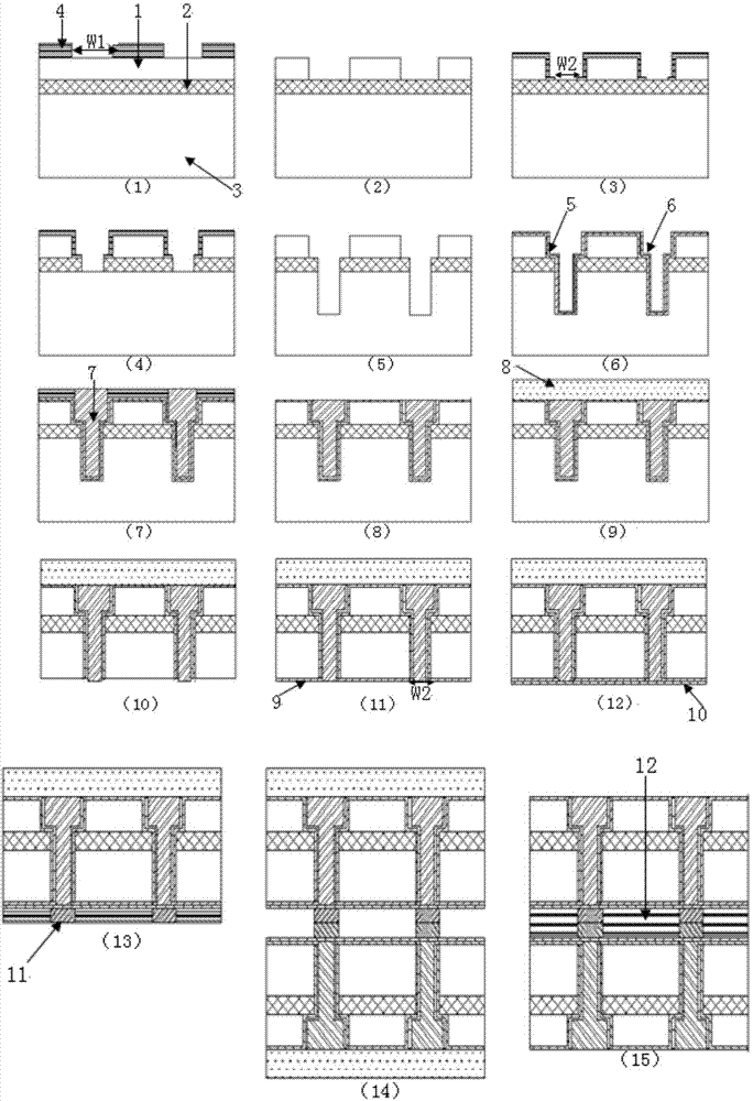
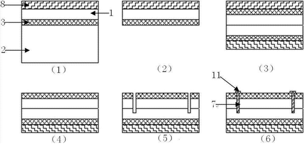
[0033] The SOI wafer substrate used is P-type silicon, and the silicon dioxide buried oxide layer is 3 thick Top Silicon 1 Thickness

[0034] (1) Coating on the surface of SOI substrate The photoresist 4 is exposed and developed to expose the window that needs to be etched on the top layer of silicon 1. The window is circular and the diameter W1 is 30 μm;

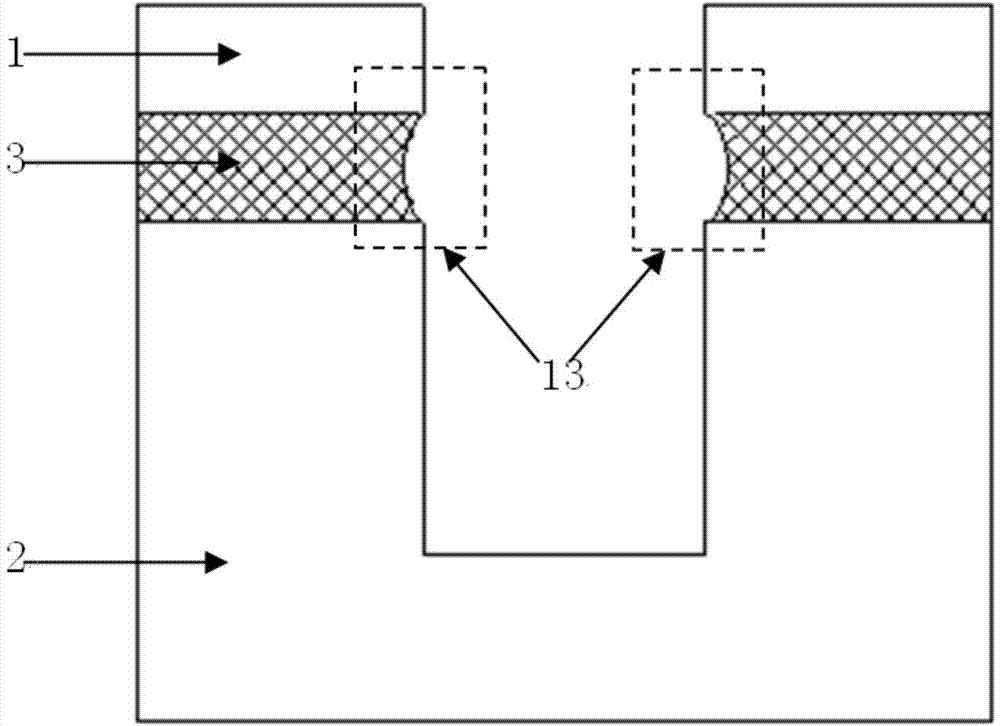
[0035] (2) Etching the top layer silicon 1 to the silicon dioxide buried oxide layer 3 stops at the window W1, and the etching depth is Then use SPM (H2SO4:H2O2:H2O=5:1:1) solution to clean and remove the photoresist 4 on the surface of the SOI wafer;

[0036] (3) Re-coat the surface of the SOI wafer with a thickness of The photoresist 4 is exposed and developed to expose the window where the silicon dioxide buried oxide layer 3 needs to be etched. The window is circular and the diameter W2 is 15 μm;

[0037] (4) Etch the silicon dioxide buried oxide layer 3 at the diameter W2 window until the upper surface of the...

Embodiment 2

[0050] The SOI wafer substrate used is P-type silicon, and the silicon dioxide buried oxide layer is 3 thick Top Silicon 1 Thickness

[0051] (1) Coating on the surface of SOI substrate The photoresist 4 is exposed and developed to expose the window that needs to be etched on the top layer of silicon 1. The window is circular and the diameter W1 is 15 μm;

[0052] (2) Etching the top layer silicon 1 to the silicon dioxide buried oxide layer 3 stops at the window W1, and the etching depth is Then use SPM (H2SO4:H2O2:H2O=5:1:1) solution to clean and remove the photoresist 4 on the surface of the SOI wafer;

[0053] (3) Re-coat the surface of the SOI wafer with a thickness of The photoresist 4 is exposed and developed to expose the window where the silicon dioxide buried oxide layer 3 needs to be etched. The window is circular and the diameter W2 is 15 μm;

[0054] (4) Etch the silicon dioxide buried oxide layer 3 at the diameter W2 window until the upper surface of the...


PUM

PropertyMeasurementUnit
thicknessaaaaaaaaaa

Abstract

The invention provides a high-reliability TSV technique based on a SOI substrate. According the technique, the existing silicon-silicon dioxide-silicon sandwich structure of the SOI substrate is not damaged, but three-dimensional integration of the SOI substrate is directly performed, so that each layer of the formed three-dimensional integrated device is provided with a buried oxide layer. The three-step etching technology is adopted to replace the existing single-step etching technology in the traditional SOI TSV technique. The method comprises the following steps: firstly etching top layer silicon, secondly etching the buried oxide layers, and at last etching bottom layer silicon, wherein the etching window of the top layer silicon is larger than that of the buried layers and the bottom layer silicon to form a horizontal etching margin on the buried oxide layer interface. The high-reliability TSV technique can avoid potential safety hazards such as the increase of electric leakage possibility and the reduction of withstand voltage, increase the possibility of the three-dimensional integrated device, greatly improve the performance of the SOI three-dimensional integrated device, and is high in the reliability.

Description

technical field [0001] The invention relates to the technical field of microelectronics. Background technique [0002] SOI devices have the characteristics of good radiation resistance, high temperature resistance, high voltage and low leakage. However, most of the TSV process methods based on SOI substrates fail to give full play to the radiation resistance, high temperature resistance, high voltage and low leakage of SOI substrates. and other advantages. As described in the document "An SOI-based three-dimensional integrated circuit technology (IEEE international SOI conference proceedings)", the TSV process method based on the SOI substrate used will make the buried oxide layer thinner when thinning the back of the wafer. As a corrosion barrier layer, all the underlying silicon is removed by chemical mechanical polishing and etching, so as to form an ultra-thin wafer with only the top silicon and buried oxide layer left. bonding (see figure 1 ). It can be seen that du...

Claims


Application Information

Patent Timeline
Patent Type & Authority Applications(China)
IPC IPC(8): H01L21/768
CPCH01L21/76805
Inventor 单光宝刘松孙有民杜欣荣张巍
Owner 珠海天成先进半导体科技有限公司
Why Eureka
Try Eureka