

Liquid crystal display panel repair method and repair system
A liquid crystal display panel and repair method technology, applied in the direction of nonlinear optics, instruments, optics, etc., can solve the problems of inability to achieve selective deposition of micro-regions, slow heating and cooling rates, structural damage, etc., to achieve environmental protection and manufacturing process Simple, Enhanced Restorative Effects
- Summary
- Abstract
- Description
- Claims
- Application Information
AI Technical Summary
Problems solved by technology
Method used
Image

Examples
Embodiment Construction
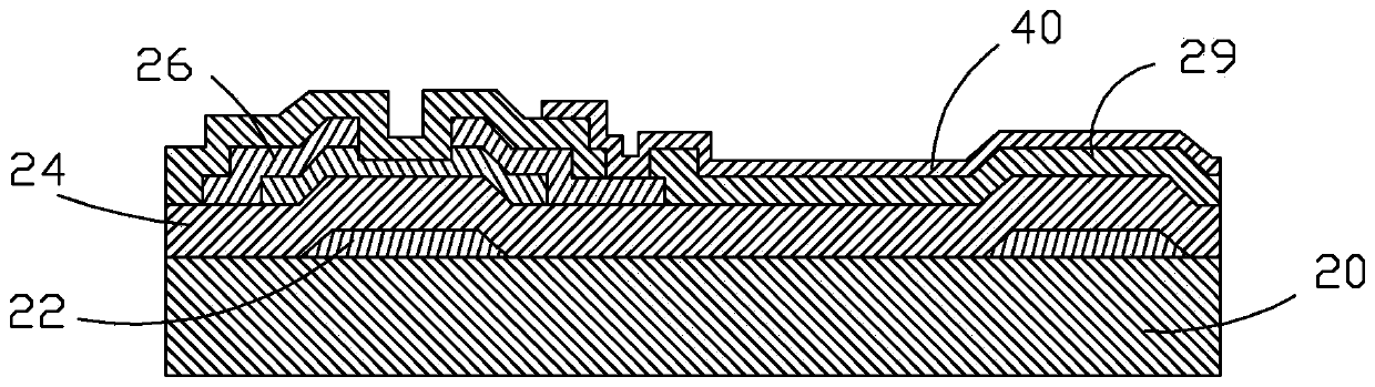
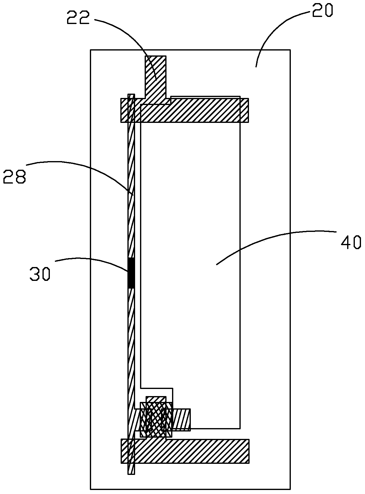
[0029] In order to further illustrate the technical means adopted by the present invention and its effects, the following describes in detail in conjunction with preferred embodiments of the present invention and accompanying drawings.
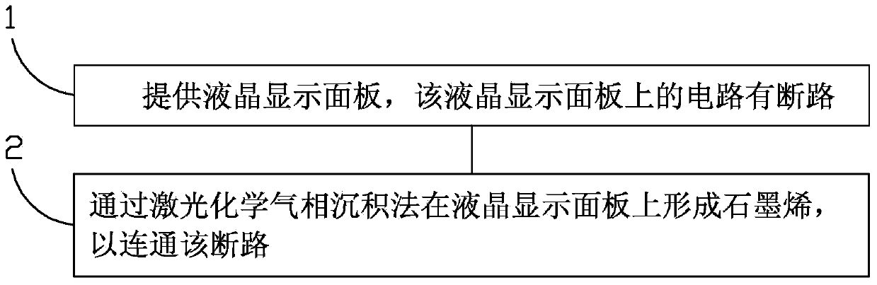
[0030] see figure 1 , the invention provides a repair method for a liquid crystal display panel, comprising the following steps:
[0031] Step 1. Provide a liquid crystal display panel, and the circuit on the liquid crystal display panel has an open circuit.
[0032] Step 2, forming graphene on the liquid crystal display panel by laser chemical vapor deposition to connect the open circuit.
[0033] In the present invention, graphene replaces the existing chromium or tungsten and deposits it at the open circuit position to repair defects. Since graphene has more excellent charge and heat transmission capabilities and excellent ductility, it solves the problem of chromium or tungsten repair due to thermal stress. Repair the defective defect, i...
PUM
 Abstract
Description
Claims
Application Information