

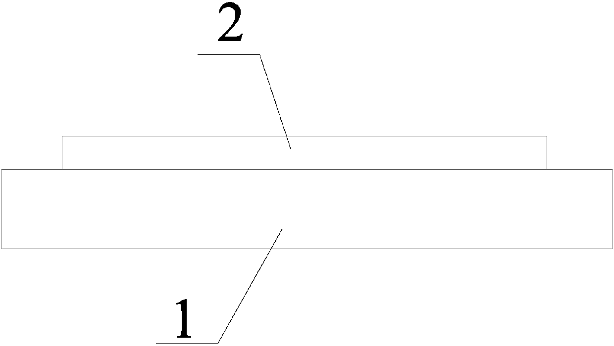
Composite structure based on Ce: YAG (yttrium aluminum garnet) wafer and production method
A composite structure and manufacturing method technology, applied in the field of optics, can solve problems such as single wavelength and reduced utility, and achieve good time characteristics, low cost, and good color rendering effect
- Summary
- Abstract
- Description
- Claims
- Application Information
AI Technical Summary
Problems solved by technology
Method used
Image

Examples
Embodiment 1
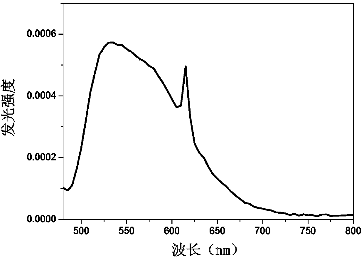
[0031] Eu:Y Plating by Sputtering 2 o 3 film, first prepare powdered Eu:Y 2 o 3 , wherein the molar concentration of Eu ions is 0.2%, and it is prepared into a bulk target by pressing method, and Eu:Y 2 o 3 The target is fixed on the cathode of the coating machine, and the Ce:YAG wafer (wherein the molar concentration of Ce ions is 0.3%) is cut and polished into the required size by the pulling method, and the cleaned Ce:YAG wafer is Fix it on the anode facing the target surface, then pump the system to high vacuum (10 -3 Pa) and then filled with argon gas of 5 Pa, apply a voltage between the cathode and the anode, start the coating, vacuumize after the coating is completed, then fill in nitrogen for cold cutting, and finally get the Eu:Y coating 2 o 3 Ce:YAG wafer composite light-emitting structure of red light-emitting film.
[0032] figure 2 Plating Eu:Y for Example 1 2 o 3 The emission spectrum of the film composite structure, as can be seen from the figure, the...
Embodiment 2
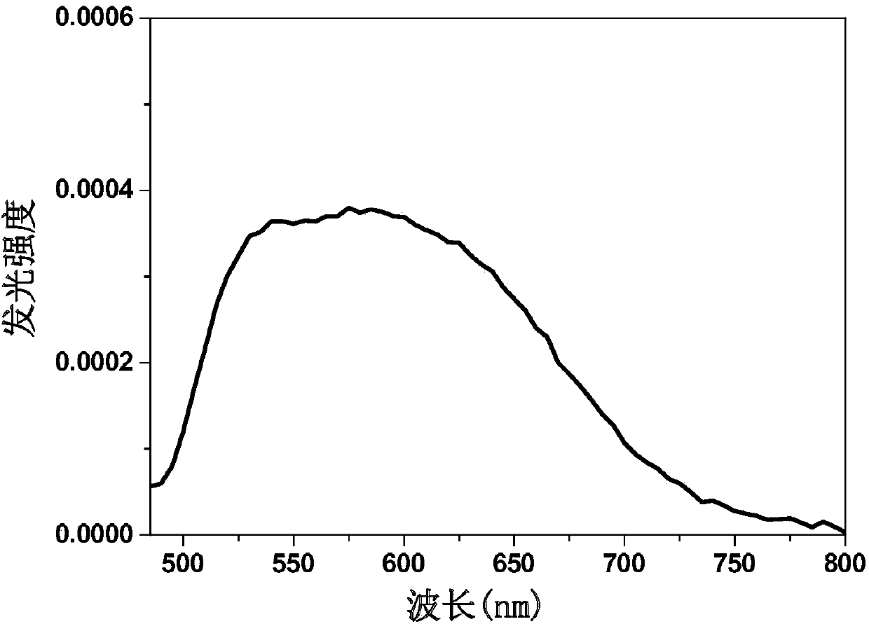
[0034] Glue-coating method to plate red phosphor film, add 0.05% by weight red phosphor to the silica gel, stir evenly, and evenly cover the Ce:YAG wafer by spraying (wherein the molar concentration of Ce ions is 0.3%, The surface of the Ce:YAG wafer is prepared by a temperature gradient method, and then baked at 120° C. for 3 hours. After the glue is cured, a Ce:YAG wafer composite light-emitting structure coated with a red phosphor film is obtained.
[0035] image 3 It is the emission spectrum diagram of the combination structure of the red-light phosphor coating film in the glue-coating mode of embodiment 2. It can be seen from the figure that the combined structure of the glue-coating red phosphor powder film coating has an emission spectrum with a width of 500nm to 750nm, and can realize the emission spectrum from green to green. Luminescence in the light to red band.
Embodiment 3
[0037] Bond the Eu:YAG wafer (where the molar concentration of Eu ions is 0.2%, prepared by the Kyroplasty method) and the Ce:YAG wafer (where the molar concentration of Ce ions is 0.5%, which is prepared by the temperature gradient method) with silica gel. Surface polishing of Ce:YAG wafer and Eu:YAG wafer to make it have good smoothness and flatness, coating the surface of Ce:YAG wafer with silica gel, covering with Eu:YAG wafer, and baking at 100°C for 3 hours, Then slowly cool down to room temperature to form a Ce:YAG and Eu:YAG wafer composite light-emitting structure.
[0038] Figure 4 It is the emission spectrum diagram of the combined structure of silica gel bonded with Eu:YAG wafer in Example 3. It can be seen from the figure that the combined structure of silica gel bonded with Eu:YAG wafer has an emission spectrum with a width of 500nm to 700nm, which can realize the emission spectrum from green light to red light. bands of glow.
PUM
 Abstract
Description
Claims
Application Information