Manufacturing method of fluorine-containing graphene decorative layer organic field effect transistor

A modified layer, graphene technology, applied in the direction of organic semiconductor devices, semiconductor/solid-state device manufacturing, electric solid-state devices, etc., can solve problems such as application limitations, achieve high photoresponsivity and photosensitivity, and improve performance.

Inactive Publication Date: 2014-06-11
UNIV OF SCI & TECH BEIJING +1
View PDF4 Cites 3 Cited by
  • Summary
  • Abstract
  • Description
  • Claims
  • Application Information

AI Technical Summary

Problems solved by technology

[0004] Graphene has been intensively studied due to its excellent properties in organic electronics (K.S. Novoselov, et al. Science, 2004, 306:666; K.S. Novoselov, et al. Nature, 2005, 438: 197.), but due to the Without a bandgap, its application in the semiconductor field is limited
Fluorine-containing graphene is a relatively young member of the graphene family, and has attracted people's interest due to its adjustable band gap (J.T.Robinson, et al. Nanoletter, 2010, 10: 3001; K.J. : 1042.), but there is no application of fluorine-containing graphene in organic phototransistors

Method used


Image

  • Manufacturing method of fluorine-containing graphene decorative layer organic field effect transistor
  • Manufacturing method of fluorine-containing graphene decorative layer organic field effect transistor

Examples


Embodiment 1

[0024] First, perform substrate pretreatment: ultrasonically clean the cut silicon wafers with clean water, secondary water, ethanol, and acetone in sequence, then put them into a mixed solution of sulfuric acid hydrogen peroxide for cleaning, and then clean them with secondary water, ethanol, and acetone Sonicate them separately, and finally dry them with nitrogen gas for later use.

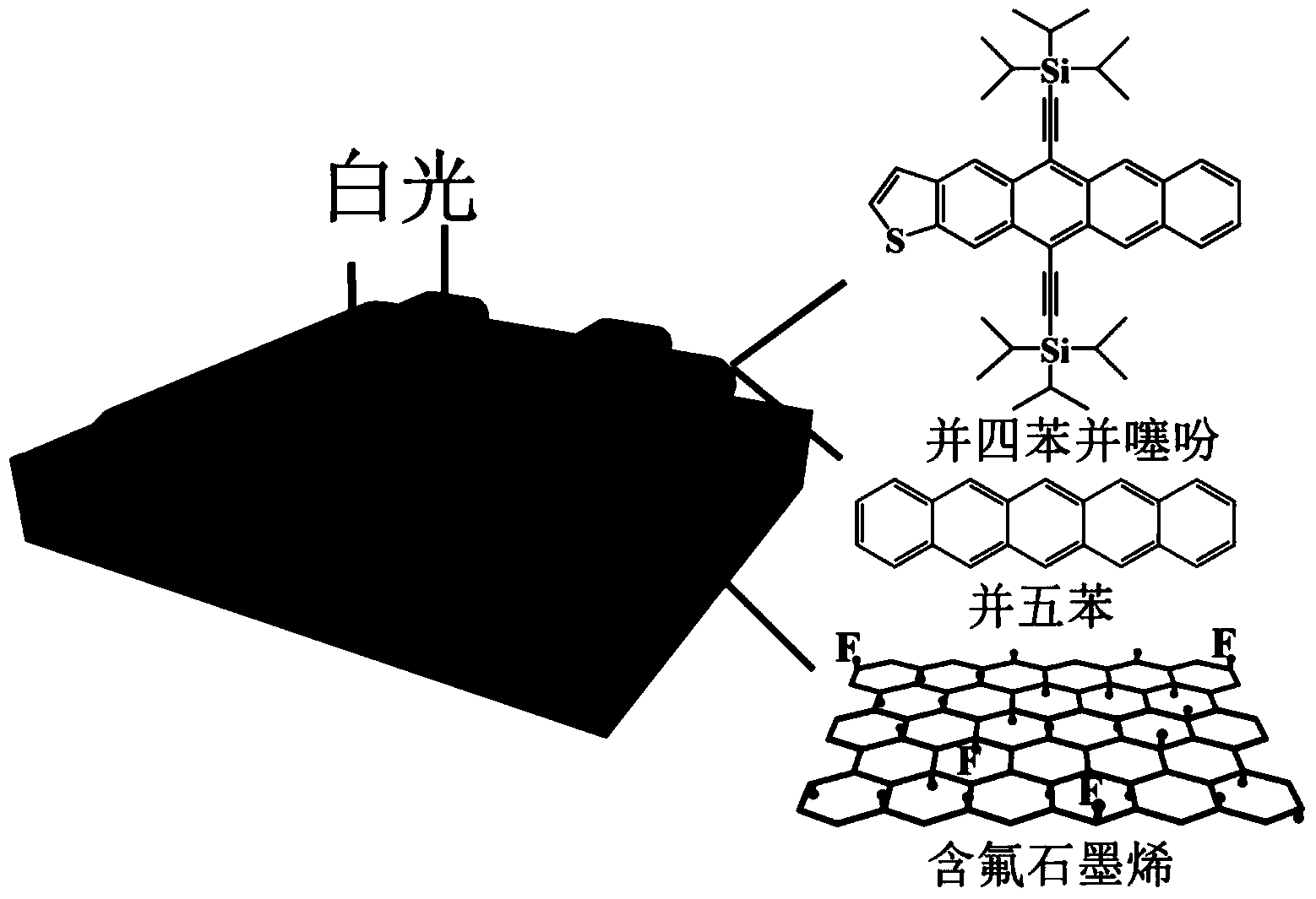
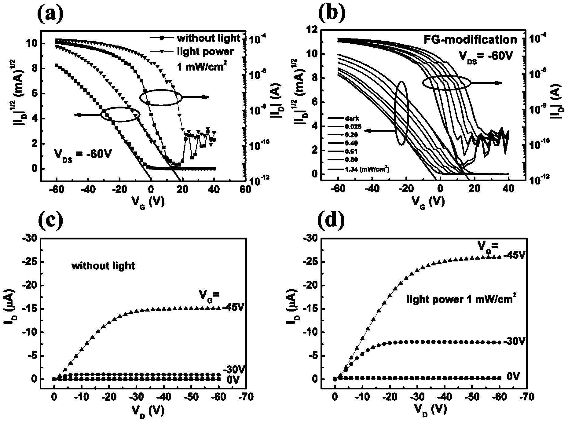
[0025] Secondly, the preparation of the modified layer: evenly spread the fluorine-containing graphene solution on a clean silicon wafer, and obtain a thin film by the method of spinning the film, and then dry the obtained film substrate in a vacuum oven at 80°C for 1 hour to obtain a modified layer substrate.

[0026] Third, the preparation of the thin film: Spread the solution of TIPSEthiotet substituted by triisopropylsilylacetylene evenly on the substrate containing the modified layer, and prepare the modified layer according to the above-mentioned method for the substrate containing the mod...

Embodiment 2

[0030] First, perform substrate pretreatment: ultrasonically clean the cut silicon wafers with clean water, secondary water, ethanol, and acetone in sequence, then put them into a mixed solution of sulfuric acid hydrogen peroxide for cleaning, and then clean them with secondary water, ethanol, and acetone Sonicate them separately, and finally dry them with nitrogen gas for later use.

[0031] Secondly, the preparation of the modified layer: evenly spread the fluorine-containing graphene solution on a clean silicon wafer, and obtain a thin film by the method of spinning the film, and then dry the obtained film substrate in a vacuum oven at 80 ° C for 2 hours to obtain a modified layer substrate.

[0032] Third, the preparation of the film: spread the pentacene solution evenly on the substrate containing the modification layer, and prepare the pentacene film containing the modification layer according to the above method for the substrate containing the modification layer.

[0...

Embodiment 3

[0036] First, perform substrate pretreatment: ultrasonically clean the cut silicon wafers with clean water, secondary water, ethanol, and acetone in sequence, then put them into a mixed solution of sulfuric acid hydrogen peroxide for cleaning, and then clean them with secondary water, ethanol, and acetone Sonicate them separately, and finally dry them with nitrogen gas for later use.

[0037] Secondly, the preparation of the modified layer: evenly spread the fluorine-containing graphene solution on a clean silicon wafer, and obtain a film by the method of spinning the film, and then dry the obtained film substrate in a vacuum oven at 50°C for 3 hours to obtain a modified layer substrate.

[0038]Third, the preparation of the thin film: Spread the solution of TIPSEthiotet substituted by triisopropylsilylacetylene evenly on the substrate containing the modified layer, and prepare the modified layer according to the above-mentioned method for the substrate containing the modified...


PUM

PropertyMeasurementUnit
thicknessaaaaaaaaaa

Abstract

The invention provides a manufacturing method of a fluorine-containing graphene decorative layer organic field effect transistor, and belongs to the field of semiconductor material devices. The manufacturing method is characterized in that fluorine-containing graphene is used as a decorative layer, organic semiconductor materials are used as a semiconductor layer, and the organic field effect transistor of a bottom-gate and bottom-electrode structure is manufactured. Through the manufacturing method, performance of the devices can be enhanced through the fluorine-containing graphene, the devices comprising the fluorine-containing graphene decorative layer with tri-isopropyl silicon acetylene substitution TIPSEthiotet and pentacene have high light responsiveness and sensibility.

Description

technical field [0001] The invention belongs to the field of semiconductor material devices, and relates to a preparation method of an organic field-effect transistor with a fluorine-containing graphene modification layer. Background technique [0002] Organic field-effect transistors have attracted extensive attention due to their great application potential in electronic fields such as sensors, memories, smart cards, electronic paper, radio frequency tags, and display drivers. In addition, organic field effect transistors have also shown great effects in other fields, such as light emission, light response, signal storage, environmental control, and medical detection. Among these functions, photoresponse includes the light-detection and signal-amplification properties of the device, which make organic field-effect transistors of great use in photoconverters. Organic field effect transistors with photoresponse function are called organic phototransistors. Compared with org...

Claims


Application Information

Patent Timeline
Patent Type & Authority Applications(China)
IPC IPC(8): H01L51/40
CPCH10K30/65H10K30/80H10K2102/00Y02E10/549
Inventor 王丽萍谢晓冬于贵张卫锋朱明山郭云龙陈鹏磊刘鸣华
Owner UNIV OF SCI & TECH BEIJING
Why Eureka
Try Eureka