Radiation-proof strengthening method for bipolar device based on geometric structure of emitter region

A technology of anti-radiation reinforcement and geometric structure, which is applied in the field of electronics, can solve the problems of large current gain damage and low anti-radiation ability of bipolar devices, and achieve simple manufacturing process steps, enhanced anti-radiation ability, and wide application foreground effect

Active Publication Date: 2014-06-18
HARBIN INST OF TECH +2
View PDF3 Cites 10 Cited by
  • Summary
  • Abstract
  • Description
  • Claims
  • Application Information

AI Technical Summary

Problems solved by technology

[0005] The present invention aims to solve the problems that the existing bipolar transistors and circuits have a large degree of damage to the current gain and low radiation resistance of bipolar devices in the space radiation environment, thereby providing a radiation resistant bipolar device based on the geometric structure of the emitter region. According to the reinforcement method

Method used


Image

  • Radiation-proof strengthening method for bipolar device based on geometric structure of emitter region
  • Radiation-proof strengthening method for bipolar device based on geometric structure of emitter region
  • Radiation-proof strengthening method for bipolar device based on geometric structure of emitter region

Examples


specific Embodiment approach 1

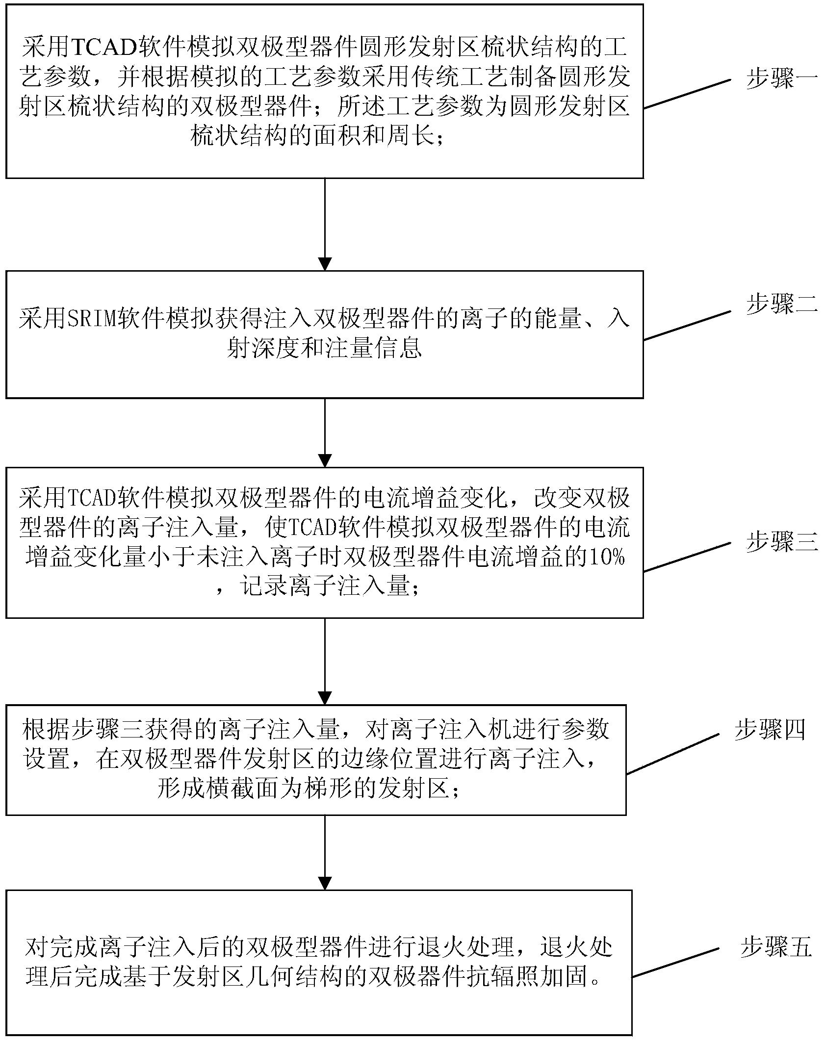
[0021] Specific implementation mode one: the following combination figure 1 Describe this embodiment mode, the radiation resistance strengthening method for bipolar devices based on the geometric structure of the emitter described in this embodiment mode, the specific steps of the method are:

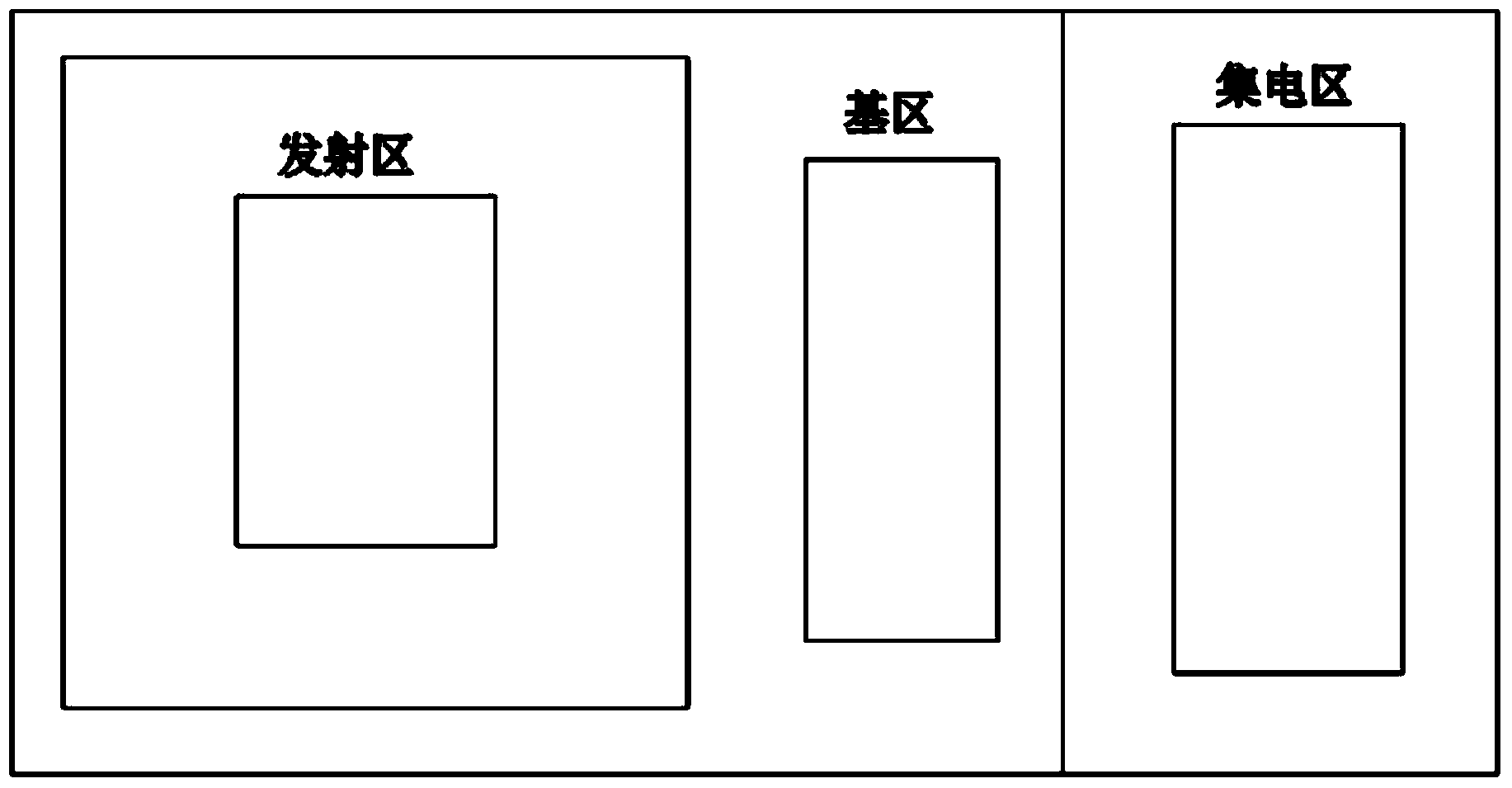
[0022] Step 1: using TCAD software to simulate the process parameters of the comb-like structure of the circular emission region of the bipolar device, and adopting the traditional process to prepare the bipolar device of the comb-shaped structure of the circular emitting region according to the simulated process parameters; the process parameters are The area and perimeter of the circular emitter comb structure;

[0023] Step 2: Using SRIM software to simulate and obtain the energy, incident depth and fluence information of ions injected into the bipolar device;

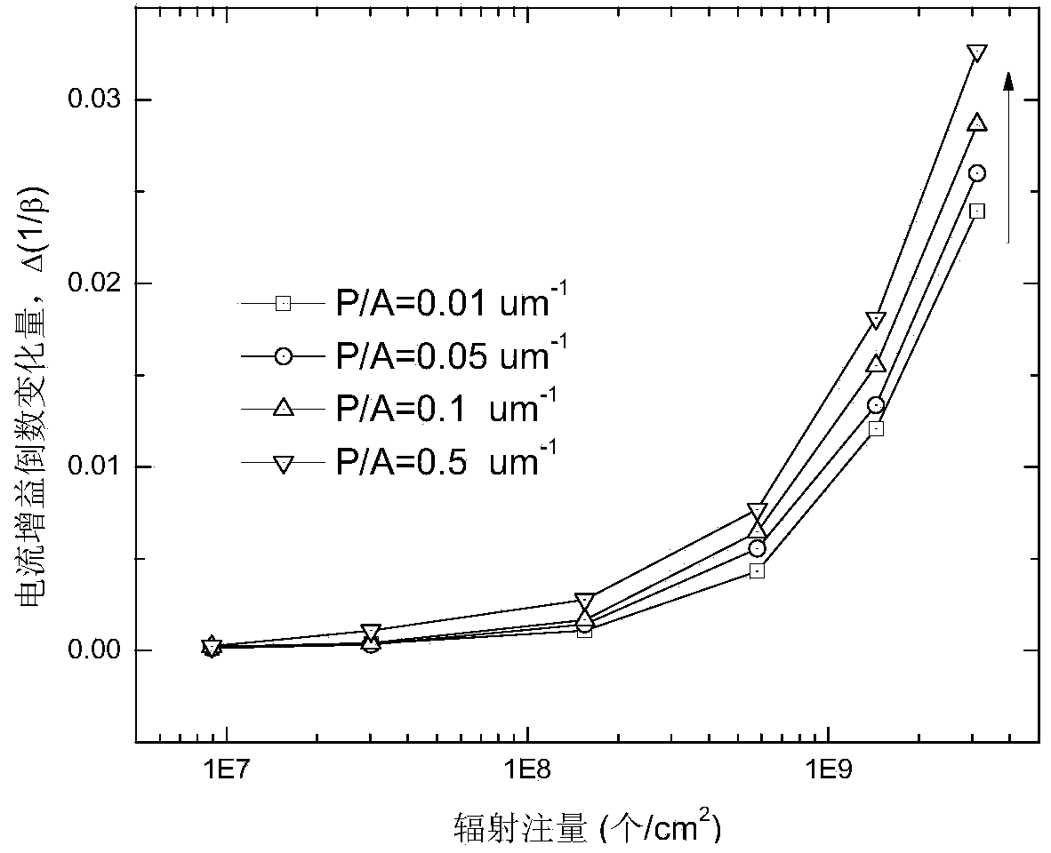
[0024] Step 3: Use TCAD software to simulate the current gain change of the bipolar device, change the ion implantation am...

specific Embodiment approach 2

[0028] Specific embodiment 2: This embodiment further limits the anti-radiation strengthening method for bipolar devices based on the geometric structure of the emission region described in the specific embodiment 1. In this embodiment, the ions described in step 2 are P-type emission regions ions or ions in the N-type emitter.

specific Embodiment approach 3

[0029] Specific implementation mode three: this implementation mode further limits the anti-radiation strengthening method for bipolar devices based on the geometric structure of the emitter region described in the second embodiment mode. In this embodiment mode, the ions in the P-type emission region are boron, Gallium ions.


PUM


Abstract

The invention relates to and is applicable to the technical field of electronics, in particular to a radiation-proof strengthening method for a bipolar device based on the geometric structure of an emitter region. The radiation-proof strengthening method aims to solve the problems that an existing bipolar junction transistor and a circuit are high in damage degree of current gain in a space radiation environment, and an existing bipolar device is low in radiation resistance ability. According to the radiation-proof strengthening method for the bipolar device, the traditional bipolar device process is reserved, and manufacturing process steps are very simple. By means of the radiation-proof strengthening method for the bipolar device, the influence of positive charges captured by oxide induced through ionizing irradiation and the interface state on performance parameters of the device can be lowered substantially by improving the geometric structure of the emitter region, and the radiation resistance ability of the bipolar device is enhanced remarkably by 2-5 times compared with that of the existing bipolar device.

Description

technical field [0001] The invention relates to the field of electronic technology. Background technique [0002] A bipolar transistor (BJT-Bipolar Junction Transistor) has good current driving capability, linearity, low noise and excellent matching characteristics, and is the basic unit of a bipolar integrated circuit. They play an important role in analog or hybrid integrated circuits and BiCMOS (Bipolar Complementary Metal Oxide Semiconductor) circuits. These bipolar transistors and circuits are widely used in spacecraft. Under the action of charged particles (protons and electrons) in space, damage to electronic devices will directly affect the reliability and life of the spacecraft. A large number of aerospace practices have shown that many aerospace accidents or failures are related to radiation damage to electronic devices, accounting for more than 40% of various spacecraft accidents or failures, and the economic losses caused are huge. Bipolar transistors and circ...

Claims


Application Information

Patent Timeline
Patent Type & Authority Applications(China)
IPC IPC(8): H01L21/328H01L21/265
CPCH01L29/0808
Inventor 李兴冀赵玉玲刘超铭刘广桥孙毅杨剑群韩力争刘艳秋李鹏伟赵运霞何世禹
Owner HARBIN INST OF TECH
Why Eureka
Try Eureka