
Preparation method and application of high-purity nanometer silicon

A nano-silicon, high-purity technology, applied in the field of electrochemical metallurgy, can solve the problems of inhibiting the large-scale application of nano-silicon, high cost, and difficulty in large-scale production, and achieve high product purity, high electrolysis efficiency, and low energy consumption. Effect

Inactive Publication Date: 2014-06-25
JIANGSU HUAFU STORAGE NEW TECH DEV +1
View PDF2 Cites 10 Cited by
  • Summary
  • Abstract
  • Description
  • Claims
  • Application Information

AI Technical Summary

Problems solved by technology

These methods have been widely used in the laboratory, but these methods are expensive and difficult to achieve large-scale production, thus greatly inhibiting the large-scale application of nano-silicon in new electronic and energy devices.

Method used


Image

  • Preparation method and application of high-purity nanometer silicon
  • Preparation method and application of high-purity nanometer silicon
  • Preparation method and application of high-purity nanometer silicon

Examples


Embodiment 1

[0032] 1.5 g of commercially available silicon dioxide powder with a purity of 99% was pressed into a silicon dioxide block with a thickness of 4 mm under a mechanical pressure of 5 MPa, and the silicon dioxide block was heated in air at 800 ° C for 0.5 hours to obtain the silicon dioxide The porosity of the block is 20%; the silica block is placed in a conductive metal current collector as the cathode, the graphite rod is used as the anode, and the molten CaCl 2 +NaCl mixed molten salt was used as the electrolyte, under the protection of argon, the electrolysis temperature was 500°C, and the cathode potential was controlled at -0.7V with a fully sealed Ag / AgCl reference electrode to perform constant potential electrolysis; after 30 minutes of electrolysis, the The electrolysis products are washed with water and 0.1mol / L HCl solution respectively, and dried after washing to obtain the required high-purity nano-silicon, the particle size of the product is 10um, and the length of...

Embodiment 2

[0034] 1 g of commercially available silicon dioxide powder with a purity of 99% was pressed into a silicon dioxide disk with a diameter of 20 mm under a mechanical pressure of 6 MPa, and the silicon dioxide disk was heated at 1200 ° C in air for 2 hours to obtain silicon dioxide The porosity of the sheet is 50%; the silicon dioxide sheet is placed in a conductive metal current collector as the cathode, the graphite rod is used as the anode, and the molten CaCl 2 As the electrolyte, under the protection of argon gas, the electrolysis temperature is 850°C, and the cathode potential is controlled at -0.8V with a fully sealed Ag / AgCl reference electrode, and constant potential electrolysis is carried out; after 10 hours of electrolysis, the electrolysis products are respectively used Water and 0.1mol / L H 2 SO 4 The solution is rinsed, and then vacuum-dried to obtain the desired high-purity nano-silicon.

Embodiment 3

[0036]20g of commercially available silicon dioxide powder with a purity of 99% was pressed into a silicon dioxide disk with a diameter of 20mm under a mechanical pressure of 10MPa, and the silicon dioxide disk was subjected to dehydration treatment in air at 100°C; The silicon dioxide sheet is placed in a conductive metal current collector as the cathode, the graphite rod is used as the anode, and the molten CaCl 2 +KCl mixed molten salt was used as the electrolyte, under the protection of argon, the electrolysis temperature was 1000 ° C, and the cathode potential was controlled at -1.0 V with a fully sealed Ag / AgCl reference electrode to perform constant potential electrolysis; after 40 hours of electrolysis, The electrolysis products are respectively washed with water and 0.1mol / L HCl solution, and then vacuum-dried to obtain the required high-purity nano-silicon.

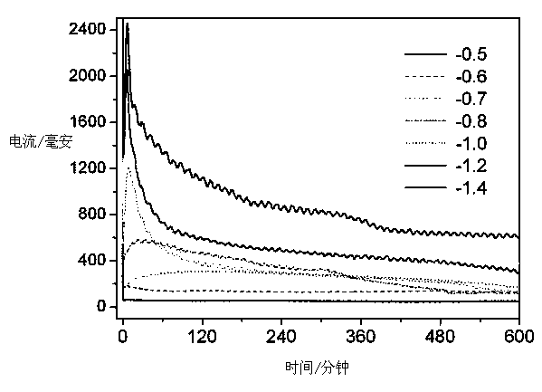
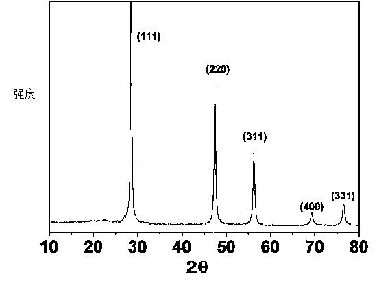
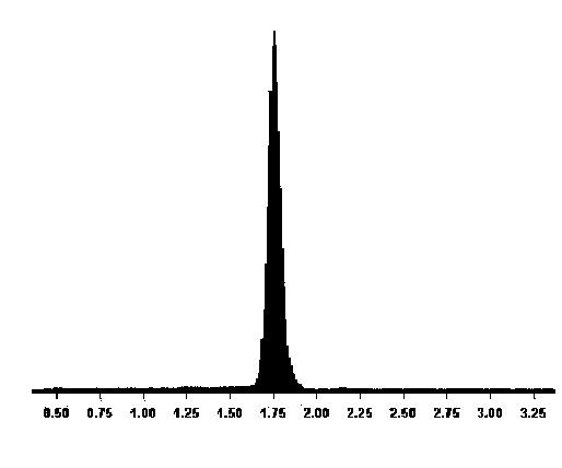
[0037] figure 1 It is a graph of cathodic current and time under different electrolysis potentials, figur...


PUM


Abstract

The invention discloses a method for preparing high-purity nanometer silicon. According to the method, calcium chloride or a calcium chloride-containing mixed fused salt is used as electrolyte, silicon dioxide or quartz is put in a metal current collector to serve as a cathode, graphite or an inert electrode is used as an anode, constant potential electrolysis is carried out under the condition that the electrolytic potential is controlled by adopting a reference electrode at a certain electrolysis temperature under the inert gas protection, thus obtaining the needed product, namely the high-purity nanometer silicon. The invention also discloses application of the high-purity nanometer silicon. The preparation method is high in electrolytic efficiency, the electrolytic efficiency is more than 70 percent, and the energy consumption is far lower than the energy consumption during silicon preparation through an industrial carbon heat method. In addition, lots of carbonic oxides are emitted in the process of preparing monatomic silicon through the industrial carbon heat method, and lots of charcoal is consumed. Moreover, the charcoal is not needed to serve as a reducing agent, an inert anode is adopted, and oxygen is discharged from the anode, so that zero emission is realized. Finally, the product obtained by the method is high in purity.

Description

[0001] technical field [0002] The invention relates to a preparation method of high-purity nano-silicon, and also relates to the application of the high-purity nano-silicon, which belongs to the technical field of electrochemical metallurgy. Background technique [0003] Elemental silicon has extensive and important applications in energy, semiconductor, organic silicon, and metallurgical industries. A large number of solar cells use high-purity silicon with a purity greater than 99.99%. At present, the production of industrial silicon is still mainly used in 1700 o C carbon thermal reduction method, in addition to high energy consumption (its energy efficiency is lower than 30%, lower overall efficiency) and serious environmental impact (carbon thermal reduction produces a large amount of greenhouse gases), the product also contains iron, aluminum, phosphorus , sulfur, carbon and other metals and non-metallic impurities, the purity of the product is not high. The produ...

Claims


Application Information

Patent Timeline
IPC IPC(8): C25B1/00
Inventor 汪的华肖巍魏迪周寿斌李超
Owner JIANGSU HUAFU STORAGE NEW TECH DEV
Learn More