Method for preparing silicon heterojunction solar cell containing composite emission layer

A silicon heterojunction and solar cell technology, which is applied in photovoltaic power generation, circuits, electrical components, etc., can solve the problems of lower battery open circuit voltage, low short-wave response of batteries, and degraded thin film microstructure, so as to reduce series resistance and parasitic Effects of absorption, reduction of interface energy band mismatch, and increase of short-wave response

Active Publication Date: 2014-07-09
捷造科技(宁波)有限公司
View PDF2 Cites 13 Cited by
  • Summary
  • Abstract
  • Description
  • Claims
  • Application Information

AI Technical Summary

Problems solved by technology

[0005] However, if the heavily doped a-Si:H material is directly used as the emitter layer of the cell, due to its many internal defects and high absorption coefficient, the parasitic absorption of the silicon heterojunction solar cell is relatively large, and the short-wave response of the cell is not good. not high, reducing the short-circuit current density
Although the wide bandgap nc-Si:H film has a wider bandgap and higher transmittance, it has a large number of high-energy particles in the high hydrogen dilution and high-power preparation conditions, and these high-energy particles bombard the intrinsic a- The Si:H film will deteriorate the microstructure of the film, reduce the passivation effect of the intrinsic a-Si:H film, and reduce the open circuit voltage of the battery

Method used


Image

  • Method for preparing silicon heterojunction solar cell containing composite emission layer
  • Method for preparing silicon heterojunction solar cell containing composite emission layer
  • Method for preparing silicon heterojunction solar cell containing composite emission layer

Examples


Embodiment 1

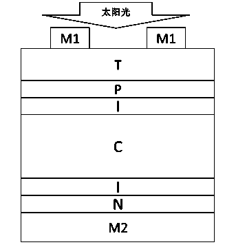
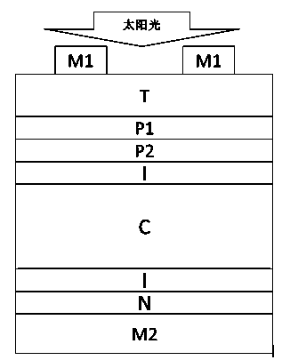
[0023] 1. Place the N-type textured Cz silicon wafer substrate in a high-vacuum plasma-enhanced chemical vapor deposition (PECVD) system, and deposit a layer of intrinsic non- Crystalline silicon I layer, and then select one side to deposit n-type amorphous silicon back field N, and then prepare to deposit p-type emitter layer on the other side.

[0024] 2. Move the sample to be processed into a 13.56MHz PECVD chamber with a background vacuum of 10 -6 Pa, the surface temperature of the sample to be processed is 180°C, and the reaction gas is introduced, and the source gas in the reaction gas is SiH 4 ; The diluent gas is H 2 ; The doping gas is TMB; the reaction gas pressure is 1.5 Torr, and the chamber electrode spacing is 20mm.

[0025] 3. Adjust the glow power density to 80mW / cm 2 , the ratio of the flow rate of various gases from [SiH 4 ]: [H 2 ]: [TMB]=1:120:1, glow deposited a 5nm a-Si:H thin film P2.

[0026] 4. Adjust the glow power density to 160mW / cm 2 , the ...

Embodiment 2

[0029] 1. Place the N-type textured Cz silicon wafer substrate in a high-vacuum plasma-enhanced chemical vapor deposition (PECVD) system, and deposit a layer of intrinsic non- Crystalline silicon I layer, and then select one side to deposit n-type amorphous silicon back field N, and then prepare to deposit p-type emitter layer on the other side.

[0030]2. Move the sample to be processed into a 13.56MHz PECVD chamber with a background vacuum of 10 -6 Pa, the surface temperature of the sample to be processed is 180°C, and the reaction gas is introduced, and the source gas in the reaction gas is SiH 4 ; The diluent gas is H 2 ; The doping gas is TMB; the reaction gas pressure is 2Torr, and the chamber electrode spacing is 20mm.

[0031] 3. Adjust the glow power density to 40mW / cm 2 , the ratio of the flow rate of various gases from [SiH 4 ]: [H 2 ]: [TMB]=1:120:2, glow deposit a 5nm a-Si:H thin film P2.

[0032] 4. Adjust the glow power density to 120mW / cm 2 , the flow r...

Embodiment 3

[0035] 1. Place the N-type textured Cz silicon wafer substrate in a high-vacuum plasma-enhanced chemical vapor deposition (PECVD) system, and deposit a layer of intrinsic non- Crystalline silicon I layer, and then select one side to deposit n-type amorphous silicon back field N, and then prepare to deposit p-type emitter layer on the other side.

[0036] 2. Move the sample to be processed into a 13.56MHz PECVD chamber with a background vacuum of 10 -6 Pa, the surface temperature of the sample to be processed is 180°C, and the reaction gas is introduced, and the source gas in the reaction gas is SiH 4 ; The diluent gas is H 2 ; The doping gas is TMB; the reaction gas pressure is 2Torr, and the chamber electrode spacing is 20mm.

[0037] 3. Adjust the glow power density to 40mW / cm 2 , the ratio of the flow rate of various gases from [SiH 4 ]: [H 2 ]: [TMB]=1:120:2.5, glow deposit a 10nm a-Si:H thin film P2.

[0038] 4. Adjust the glow power density to 120mW / cm 2 , the fl...


PUM

PropertyMeasurementUnit
thicknessaaaaaaaaaa
thicknessaaaaaaaaaa
electrical conductivityaaaaaaaaaa

Abstract

The invention provides a method for preparing a silicon heterojunction solar cell containing a composite emission layer. The method includes the steps that an amorphous silicon back field N is deposited on one face of a substrate C on which a double-faced intrinsic amorphous silicon passivation layer I is deposited, an amorphous silicon layer P2 with the uniform structure is prepared on the face opposite to the amorphous silicon back field N under the conditions that doping concentration, hydrogen dilution and power density are low, a nanocrystalline silicon layer P1 with the uniform structure is prepared under the conditions that the doping concentration, the hydrogen dilution and the power density are improved, and an amorphous silicon / nanocrystalline silicon composite structure formed by the two silicon films serves as the emission layer of the silicon heterojunction solar cell. Materials have the advantages of being high in transmittance and conductivity through the structure, on the basis, the passivation effect of the surface of crystalline silicon can be improved, short wave response and output characteristics of the cell are improved, and the method for preparing the silicon heterojunction solar cell is simple and easy to carry out.

Description

[0001] technical field [0002] The invention relates to a method for preparing a silicon heterojunction solar cell, in particular to a method for preparing a solar cell containing a P-type amorphous silicon / nanocrystalline silicon composite emission layer. Background technique [0003] Photovoltaic power generation is one of the internationally recognized effective ways to solve the problems of energy shortage and environmental pollution. The carrier of photovoltaic power generation is solar cells, and the key to making solar cells an important part of future energy is to reduce the cost of photovoltaic power generation to the same level as conventional energy. Silicon heterojunction solar cells have attracted widespread attention due to their high conversion efficiency, low energy consumption in the preparation process, and relatively cheap production costs. [0004] Silicon heterojunction solar cells usually use doped a-Si:H film as the emitter layer of the cell. Compare...

Claims


Application Information

Patent Timeline
Patent Type & Authority Applications(China)
IPC IPC(8): H01L31/072H01L31/20
CPCH01L31/0725H01L31/202Y02E10/50Y02P70/50
Inventor 张晓丹王奉友魏长春许盛之赵颖
Owner 捷造科技(宁波)有限公司
Why Eureka
Try Eureka