
Eureka
For R&D, Eureka makes reading and utilizing patents & technical documents easy.
Eureka AIR
Designed for self-driven R&D workflows. Generate viable solutions, solve complex R&D challenges, empower your innovation with AI.

Eureka Materials
Designed for material experts only. Revolutionize your material R&D, from search, analyze, to developing new materials.

TechResearch
Generate reliable direction feasibility study reports for your R&D in just a few steps.

TechSeek
Discover and master advanced knowledge NOW. Basics, ideas, possibilities, all at once.

TechMind
As an expert in R&D Theories, TechMind can generates customized viable solutions instantly.

TechRisk
Analyze your overall solution with one click, know your potential R&D risks in advance.

TechMonitor
Get weekly tech updates, stay abreast of the latest tech innovations and key insights.
Organic electroluminescence device and manufacturing method thereof
An electroluminescence device and electroluminescence technology, which are applied in the manufacturing of organic semiconductor devices, electric solid state devices, semiconductor/solid state devices, etc., can solve the problems of difficulty in finding and designing hole blocking materials, and achieve easy operation and improve luminous efficiency. , the effect of low raw material prices
- Summary
- Abstract
- Description
- Claims
- Application Information
AI Technical Summary
Problems solved by technology
Method used
Image

Examples
Embodiment 1
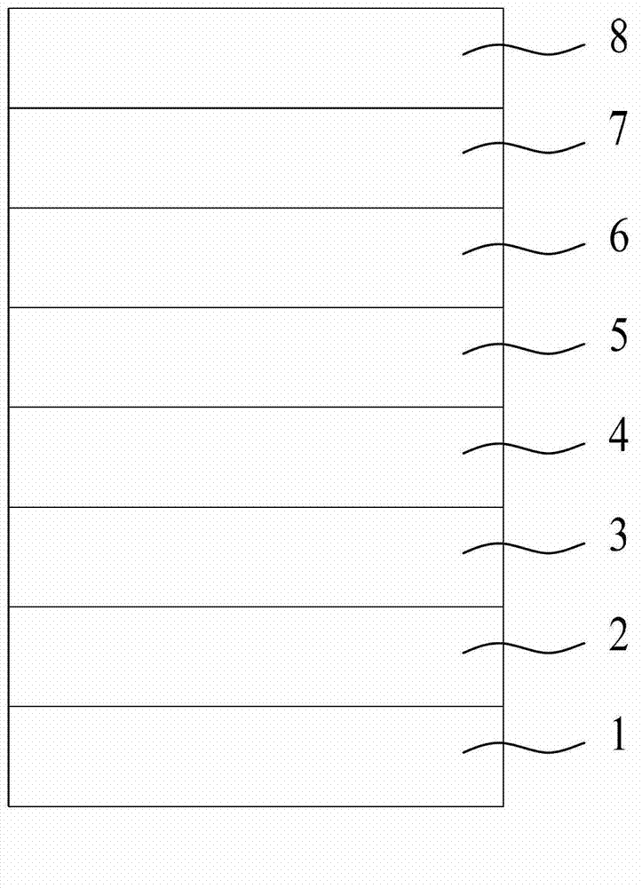
[0046] A method for preparing an organic electroluminescent device, comprising the following steps:
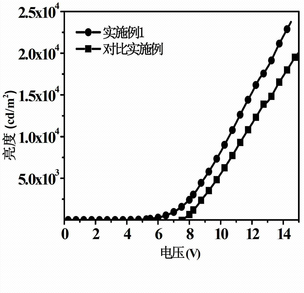
[0047] (1) The conductive anode 1 is made of indium tin oxide glass (ITO). First, the conductive anode 1 is subjected to photolithography treatment, and then cut into 2×2cm 2 The square conductive anode of the glass is ultrasonically cleaned with detergent, deionized water, acetone, ethanol, and isopropanol for 15 minutes each to remove organic pollutants on the glass surface, cleaned and air-dried; Hole injection layer 2, hole transport layer 3, light emitting layer 4; wherein the material of the hole injection layer is WO 3 , the thickness is 50nm, and the pressure used in evaporation is 5×10 -3 Pa, the evaporation rate is 1nm / s; the material of the hole transport layer is TCTA, the thickness is 40nm, and the pressure used in the evaporation is 5×10 -3 Pa, the evaporation rate is 0.1nm / s; the material of the light-emitting layer is ADN, the thickness is 10nm, and the press...
Embodiment 2
[0053] A method for preparing an organic electroluminescent device, comprising the following steps:
[0054] (1) The conductive anode is made of aluminum-doped zinc oxide glass (AZO). First, the conductive anode is photolithographically processed, and then cut into 2×2cm 2 The square conductive anode of the glass is ultrasonically cleaned with detergent, deionized water, acetone, ethanol, and isopropanol for 15 minutes each to remove organic pollutants on the glass surface, cleaned and air-dried; then holes are sequentially evaporated on the conductive anode Injection layer, hole transport layer, light emitting layer. Wherein, the material of the hole injection layer is V 2 o 5 , the thickness is 80nm, and the pressure used in evaporation is 2×10 -3 Pa, the evaporation rate is 5nm / s; the material of the hole transport layer is TAPC, the thickness is 60nm, and the pressure used in the evaporation is 2×10 -3 Pa, the evaporation rate is 0.5nm / s; the material of the light-emit...
Embodiment 3
[0060] A method for preparing an organic electroluminescent device, comprising the following steps:
[0061] (1) The conductive anode is made of indium-doped zinc oxide glass (IZO). First, the conductive anode is photolithographically processed, and then cut into 2×2cm 2 The square conductive anode of the glass is ultrasonically cleaned with detergent, deionized water, acetone, ethanol, and isopropanol for 15 minutes each to remove organic pollutants on the glass surface, cleaned and air-dried; then holes are sequentially evaporated on the conductive anode Injection layer, hole transport layer, light emitting layer. Wherein, the material of the hole injection layer is MoO 3 , the thickness is 40nm, and the pressure used in evaporation is 5×10 -4 Pa, the evaporation rate is 3nm / s; the material of the hole transport layer is TCTA, the thickness is 45nm, and the pressure used in the evaporation is 5×10 -4 Pa, the evaporation rate is 0.3nm / s; the material of the light-emitting ...
PUM
| Property | Measurement | Unit |
|---|---|---|
| thickness | aaaaa | aaaaa |
| thickness | aaaaa | aaaaa |
| thickness | aaaaa | aaaaa |
Abstract
Description
Claims
Application Information
 - R&D Engineer
- R&D Manager
- IP Professional
- Industry Leading Data Capabilities
- Powerful AI technology
- Patent DNA Extraction
Browse by: Latest US Patents, China's latest patents, Technical Efficacy Thesaurus, Application Domain, Technology Topic, Popular Technical Reports.
© 2024 PatSnap. All rights reserved.Legal|Privacy policy|Modern Slavery Act Transparency Statement|Sitemap|About US| Contact US: help@patsnap.com