High-energy pulse-type magnetron sputtering method and magnetron sputtering device

A magnetron sputtering and pulse sputtering technology, which is applied in sputtering plating, ion implantation plating, metal material coating process, etc., can solve the problem of rough coating surface, poor coating finish, and poor adhesion of thick ion coating and other problems, to achieve the effect of improving uniformity and other characteristics, precise adjustment methods, and eliminating thermal effects

Inactive Publication Date: 2014-07-23
HONG KONG PRODUCTIVITY COUNCIL +1
View PDF4 Cites 17 Cited by
  • Summary
  • Abstract
  • Description
  • Claims
  • Application Information

AI Technical Summary

Problems solved by technology

Due to the limited ionization percentage used in the plasma plating technology, the general ionization percentage is greater than 10%, and the thick ion plating layer with a thickness greater than 2 microns produced by the conventional magnetron sputtering method has poor adhesion.
In addition, the coating prepared by cathodic arc evaporation has a rough surface due to the ejection of large particles, and the finish of the coating is not good.

Method used


Image

  • High-energy pulse-type magnetron sputtering method and magnetron sputtering device
  • High-energy pulse-type magnetron sputtering method and magnetron sputtering device
  • High-energy pulse-type magnetron sputtering method and magnetron sputtering device

Examples


Embodiment 1

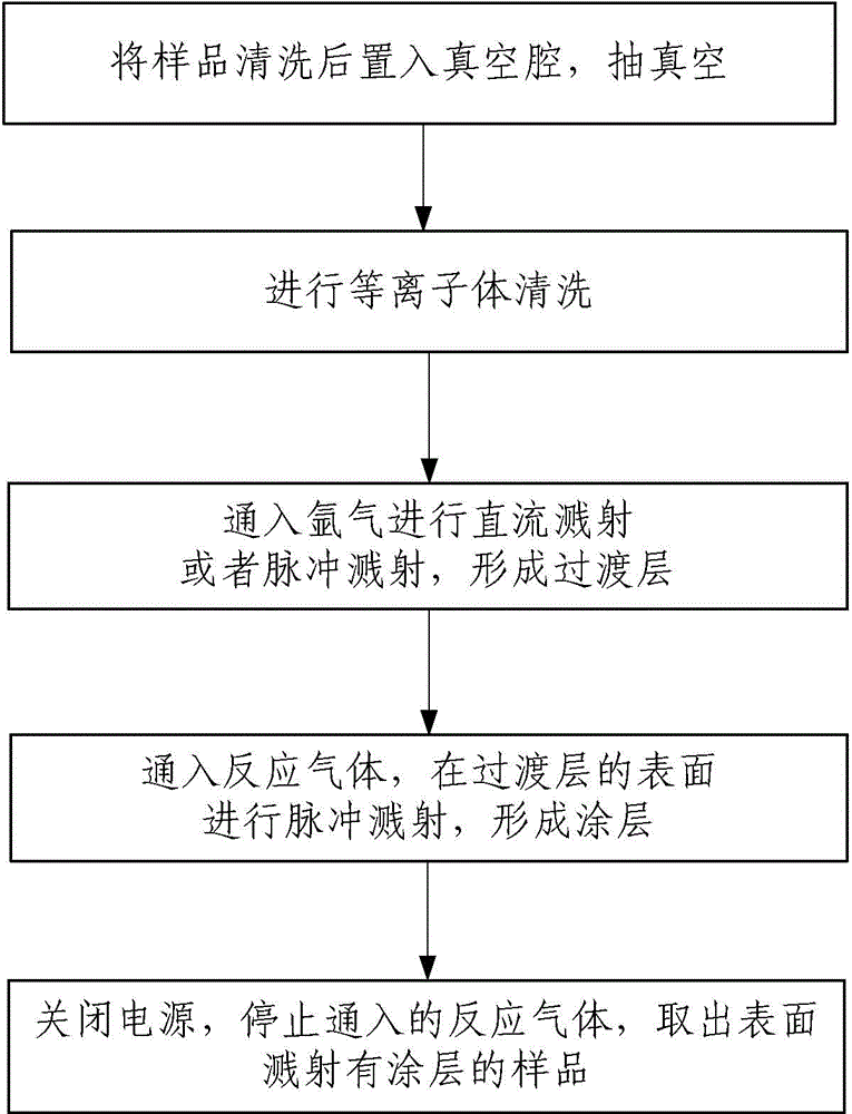
[0042] The following examples illustrate the high-energy pulsed magnetron sputtering method of the present invention by taking the sputtering TiN coating as an example, which specifically includes the following steps:

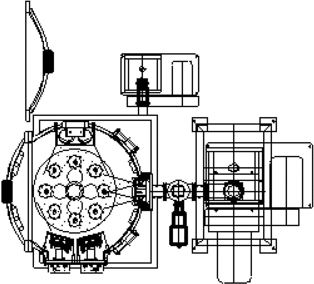
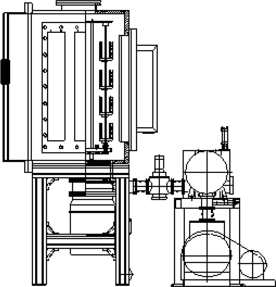
[0043] Step 1: Install the Ti target on the sputtering cathode; select a metal, plastic or semiconductor substrate as a sample, put it into the vacuum chamber 4 after cleaning, degreasing, and drying, and install it on the workpiece; vacuum the vacuum chamber 4 Vacuum, so that the gas pressure in the vacuum chamber 4 is lower than 1E-4mbar.

[0044] Step 2: Add argon gas Ar, the gas flow rate of the argon gas is 120 sccm, until the entire sputtering process is over; the sample is plasma cleaned, and the bias voltage is applied to the sample for about 10 minutes (value range), and the bias power is set to bias The pulse time of piezoelectric power supply is 0.8μs, the pulse frequency of bias power supply is 240kHz, the voltage of bias power supply is 50V, and th...

Embodiment 2

[0053] The following examples illustrate the high-energy pulsed magnetron sputtering method of the present invention by taking the sputtering CrN coating as an example, which specifically includes the following steps:

[0054] Step 1: Clean, degrease, and dry the sample to be coated and put it into the vacuum chamber 4, and install the cathode target in the vacuum chamber 4, and then perform vacuum pumping to make the gas in the vacuum chamber 4 Pressure below 8E-5 mbar. The cathode target is a Cr target, and the purity of the target is greater than or equal to 99%.

[0055] Step 2: fill in argon gas, set the flow rate of the gas to 120 sccm, perform plasma cleaning on the sample, apply a bias voltage to the sample for 20 minutes, and set the bias voltage power supply to a power pulse time of 0.4 when applying the bias voltage μs, the pulse frequency of the bias power supply is 5kHz, the voltage of the bias power supply is 20V, and the current of the bias power supply is 0.1A...

Embodiment 3

[0060] The following examples illustrate the high-energy pulsed magnetron sputtering method of the present invention by taking the sputtering TiAlCN coating as an example, which specifically includes the following steps:

[0061] Step 1: Clean, degrease, and dry the sample to be coated and put it into the vacuum chamber 4, and install the cathode target in the vacuum chamber 4, wherein the target is a bipolar target, which is divided into Ti target and The Al target is then evacuated to make the gas pressure in the vacuum chamber 4 lower than 1E-4 mbar after evacuation. The purity of the target is greater than or equal to 99%.

[0062] Step 2: fill in argon gas, set the flow rate of the gas to 80 sccm, perform plasma cleaning on the sample, apply a bias voltage to the sample for 10 minutes, and set the bias power supply to a power pulse time of 2.3 μs when applying the bias voltage, The pulse frequency of the bias power is 350kHz, the voltage of the bias power is 50V, and the...


PUM

PropertyMeasurementUnit
thicknessaaaaaaaaaa
thicknessaaaaaaaaaa

Abstract

The invention provides a high-energy pulse-type magnetron sputtering method and a magnetron sputtering device. The method includes: cleaning a sample, putting the sample into a vacuum chamber and vacuumizing the vacuum chamber; feeding argon to perform plasma cleaning for the sample; feeding argon as a sputtering gas and performing direct current sputtering or pulse sputtering on the surface of the sample to form a transition layer; feeding a reaction gas and performing pulse sputtering on the surface of the transition layer to form a coating; and closing a sputtering cathode, stopping feeding of the reaction gas, and taking out the sample the surface of which is sputtered with the coating. Compared with traditional magnetron sputtering technologies, the gas participating in the reaction and the ionization rate of the target material particles are increased, thus largely improving the density, uniformity, and other properties of the formed film, eliminating the heating effect in manufacturing processes of a thick coating, and reducing the internal stress for forming the film. The magnetron sputtering method adjusts the color through a method of adjusting the gas flow rate, and a pulse waveform adjusting method of the magnetron sputtering method is more accurate and wider in scope than traditional methods.

Description

technical field [0001] The invention belongs to the technical field of coating preparation, and in particular relates to a high-energy pulse magnetron sputtering method and a magnetron sputtering device. Background technique [0002] At present, in Hong Kong, more than 300 manufacturing factories use ion plating technology to prepare clocks and watches, mobile phone cases, auto parts, knives and molds. Usually, the thickness of the coating prepared by ion plating technology is generally less than 2 microns. In recent years, major brand companies have devoted themselves to increasing the coating thickness of their products, which is generally required to be greater than 2 microns, in order to improve their high-tech image. Due to the limited ionization percentage used in the plasma plating technology, generally the ionization percentage is greater than 10%, and the thick ion plating layer with a thickness greater than 2 microns produced by the conventional magnetron sputteri...

Claims


Application Information

Patent Timeline
Patent Type & Authority Applications(China)
IPC IPC(8): C23C14/35
Inventor 卢伟贤谢贯尧张忠祥易敏龙刘耀鸿
Owner HONG KONG PRODUCTIVITY COUNCIL
Why Eureka
Try Eureka